ZHCSFO3D November 2016 – August 2021 LM5170-Q1
PRODUCTION DATA
- 1 特性
- 2 应用
- 3 说明
- 4 Revision History
- 5 说明(续)
- 6 Pin Configuration and Functions
- 7 Specifications
-
8 Detailed Description
- 8.1 Overview
- 8.2 Functional Block Diagram
- 8.3
Feature Description
- 8.3.1 Bias Supply (VCC, VCCA)
- 8.3.2 Undervoltage Lockout (UVLO) and Master Enable or Disable
- 8.3.3 High Voltage Input (VIN, VINX)
- 8.3.4 Current Sense Amplifier
- 8.3.5 Control Commands
- 8.3.6 Channel Current Monitor (IOUT1, IOUT2)
- 8.3.7 Cycle-by-Cycle Peak Current Limit (IPK)
- 8.3.8 Error Amplifier
- 8.3.9 Ramp Generator
- 8.3.10 Soft Start
- 8.3.11 Gate Drive Outputs, Dead Time Programming and Adaptive Dead Time (HO1, HO2, LO1, LO2, DT)
- 8.3.12 PWM Comparator
- 8.3.13 Oscillator (OSC)
- 8.3.14 Synchronization to an External Clock (SYNCIN, SYNCOUT)
- 8.3.15 Diode Emulation
- 8.3.16 Power MOSFET Failure Detection and Failure Protection (nFAULT, BRKG, BRKS)
- 8.3.17 Overvoltage Protection (OVPA, OVPB)
- 8.4 Device Functional Modes
- 8.5 Programming
-
9 Application and Implementation
- 9.1 Application Information
- 9.2
Typical Application
- 9.2.1
60-A, Dual-Phase, 48-V to 12-V Bidirectional Converter
- 9.2.1.1 Design Requirements
- 9.2.1.2
Detailed Design Procedure
- 9.2.1.2.1 Determining the Duty Cycle
- 9.2.1.2.2 Oscillator Programming
- 9.2.1.2.3 Power Inductor, RMS and Peak Currents
- 9.2.1.2.4 Current Sense (RCS)
- 9.2.1.2.5 Current Setting Limits (ISETA or ISETD)
- 9.2.1.2.6 Peak Current Limit
- 9.2.1.2.7 Power MOSFETS
- 9.2.1.2.8 Bias Supply
- 9.2.1.2.9 Boot Strap
- 9.2.1.2.10 RAMP Generators
- 9.2.1.2.11 OVP
- 9.2.1.2.12 Dead Time
- 9.2.1.2.13 IOUT Monitors
- 9.2.1.2.14 UVLO Pin Usage
- 9.2.1.2.15 VIN Pin Configuration
- 9.2.1.2.16 Loop Compensation
- 9.2.1.2.17 Soft Start
- 9.2.1.2.18 ISET Pins
- 9.2.1.3 Application Curves
- 9.2.1
60-A, Dual-Phase, 48-V to 12-V Bidirectional Converter
- 10Power Supply Recommendations
- 11Layout
- 12Device and Documentation Support
- 13Mechanical, Packaging, and Orderable Information
8.3.11 Gate Drive Outputs, Dead Time Programming and Adaptive Dead Time (HO1, HO2, LO1, LO2, DT)
Each channel of the LM5170-Q1 has a robust 5-A (peak) half bridge driver to drive external N-channel power MOSFETs. As shown in Figure 8-8, the low-side drive is directly powered by VCC, and the high-side driver by the bootstrap capacitor CBT. During the on-time of the low-side driver, the SW pin is pulled down to PGND and CBT is charged by VCC through the boot diode DBT. TI recommends selecting a 0.1-µF or larger ceramic capacitor for CBT, and an ultra-fast diode of 1 A and 100-V ratings for DBT. TI also strongly recommends users to add a 2-Ω to 5-Ω resistor (RBT) in series with DBT to limit the surge charging current and improve the noise immunity of the high-side driver.
 Figure 8-8 Bootstrap Circuit for High-Side Bias Supply
During start-up in buck mode, CBT may not be charged initially; the LM5170-Q1 then holds off the high-side driver outputs (HO1 and HO2) and sends LO pulses of 200-ns width in consecutive cycles to pre-charge CBT. When the boot voltage is greater than the 6.5-V boot UV threshold, the high-side drivers output PWM signals at the HO1 and HO2 pins for normal switching action.
During start-up in boost mode, CBT is naturally charged by the normal turnon of the low side MOSFET, therefore there is no such 200-ns pre-charge pulse at the LO pins.
To prevent shoot-through between the high-side and low-side power MOSFETs on the same half bridge leg, two types of dead time schemes can be chosen with the DT pin: the programmable dead time or built-in adaptive dead time.
To program the dead time, place a resistor RDT across the DT and AGND pins as shown in Figure 8-9.
The dead time tDT as depicted in Figure 8-10 is determined by Equation 15:
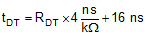
Note that this equation is valid for programming tDT between 20 ns and 250 ns. When the power MOSFET is connected to the gate drive, its gate input capacitance CISS becomes a load of the gate drive output, and the HO and LO slew rate are reduced, leading to a reduced effective tDT between the high- and low-side MOSFETs. The user should evaluate the effective tDT to make sure it is adequate to prevent shoot-through between the high- and low-side MOSFETs.
When the DT programmability is not used, simply connect the DT pin to VCC as shown in Figure 8-11, to activate the built-in adaptive dead time. The adaptive dead time is implemented by real time monitoring of a driver’s output (either HO or LO) by the other driver (LO or HO) of the same half bridge switch leg, as shown in Figure 8-11 and Figure 8-12. Only when a driver’s output voltage falls below 1.25 V does the other driver starts turnon. The effectiveness of adaptive dead time is greatly reduced if a series gate resistor is used, or if the PCB traces of the gate drive have excessive impedance due to poor layout design.
") Figure 8-9 Dead Time Programming With DT Pin (Only One Channel is Shown)
Figure 8-9 Dead Time Programming With DT Pin (Only One Channel is Shown)") Figure 8-10 Gate Drive Dead Time (Only One Channel is Shown)
Figure 8-10 Gate Drive Dead Time (Only One Channel is Shown)") Figure 8-11 Dead Time Programming With DT Pin (Only One Channel is Shown)
Figure 8-11 Dead Time Programming With DT Pin (Only One Channel is Shown)") Figure 8-12 Adaptive Dead Time (Only One Channel is Shown)
Figure 8-12 Adaptive Dead Time (Only One Channel is Shown)