ZHCSFO3D November 2016 – August 2021 LM5170-Q1
PRODUCTION DATA
- 1 特性
- 2 应用
- 3 说明
- 4 Revision History
- 5 说明(续)
- 6 Pin Configuration and Functions
- 7 Specifications
-
8 Detailed Description
- 8.1 Overview
- 8.2 Functional Block Diagram
- 8.3
Feature Description
- 8.3.1 Bias Supply (VCC, VCCA)
- 8.3.2 Undervoltage Lockout (UVLO) and Master Enable or Disable
- 8.3.3 High Voltage Input (VIN, VINX)
- 8.3.4 Current Sense Amplifier
- 8.3.5 Control Commands
- 8.3.6 Channel Current Monitor (IOUT1, IOUT2)
- 8.3.7 Cycle-by-Cycle Peak Current Limit (IPK)
- 8.3.8 Error Amplifier
- 8.3.9 Ramp Generator
- 8.3.10 Soft Start
- 8.3.11 Gate Drive Outputs, Dead Time Programming and Adaptive Dead Time (HO1, HO2, LO1, LO2, DT)
- 8.3.12 PWM Comparator
- 8.3.13 Oscillator (OSC)
- 8.3.14 Synchronization to an External Clock (SYNCIN, SYNCOUT)
- 8.3.15 Diode Emulation
- 8.3.16 Power MOSFET Failure Detection and Failure Protection (nFAULT, BRKG, BRKS)
- 8.3.17 Overvoltage Protection (OVPA, OVPB)
- 8.4 Device Functional Modes
- 8.5 Programming
-
9 Application and Implementation
- 9.1 Application Information
- 9.2
Typical Application
- 9.2.1
60-A, Dual-Phase, 48-V to 12-V Bidirectional Converter
- 9.2.1.1 Design Requirements
- 9.2.1.2
Detailed Design Procedure
- 9.2.1.2.1 Determining the Duty Cycle
- 9.2.1.2.2 Oscillator Programming
- 9.2.1.2.3 Power Inductor, RMS and Peak Currents
- 9.2.1.2.4 Current Sense (RCS)
- 9.2.1.2.5 Current Setting Limits (ISETA or ISETD)
- 9.2.1.2.6 Peak Current Limit
- 9.2.1.2.7 Power MOSFETS
- 9.2.1.2.8 Bias Supply
- 9.2.1.2.9 Boot Strap
- 9.2.1.2.10 RAMP Generators
- 9.2.1.2.11 OVP
- 9.2.1.2.12 Dead Time
- 9.2.1.2.13 IOUT Monitors
- 9.2.1.2.14 UVLO Pin Usage
- 9.2.1.2.15 VIN Pin Configuration
- 9.2.1.2.16 Loop Compensation
- 9.2.1.2.17 Soft Start
- 9.2.1.2.18 ISET Pins
- 9.2.1.3 Application Curves
- 9.2.1
60-A, Dual-Phase, 48-V to 12-V Bidirectional Converter
- 10Power Supply Recommendations
- 11Layout
- 12Device and Documentation Support
- 13Mechanical, Packaging, and Orderable Information
8.3.13 Oscillator (OSC)
The LM5170-Q1 oscillator frequency is set by the external resistor ROSC connected between the OSC pin and AGND, as shown in Figure 8-13. The OSC pin must never be left open whether or not an external clock is present. To set a desired oscillator frequency FOSC, ROSC is approximately determined by Equation 17:
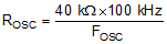
ROSC must be placed as close as possible to the OSC and AGND pins. Take the tolerance of the external resistor and the frequency tolerance indicated in Section 7.5 into account when determining the worst case operating frequency.
The LM5170-Q1 also includes a Phase-Locked Loop (PLL) circuit to manage multiphase interleaving phase angle as well as the synchronization to the external clock applied at the SYNCIN pin. When no external clock is present, the converter operates at the oscillator frequency given by Equation 17. If an external clock signal of a frequency within ± 20% of FSW is applied (see Section 8.3.14), the converter will switch at the frequency of the external clock FEX_CLK, namely Equation 18:
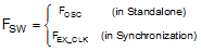
Two internal clock signals CLK1 and CLK2 are produced to control the interleaving operation of CH-1 and CH-2, respectively. The third clock signal is output at the SYNCOUT pin. All these three clock signals run at the same frequency of FSW. The phase angles among these three clock signals are controlled by the state of the OPT pin. See Section 8.4.1 for details.
 Figure 8-13 Oscillator and Interleaving Clock Programming