ZHCSFO3D November 2016 – August 2021 LM5170-Q1
PRODUCTION DATA
- 1 特性
- 2 应用
- 3 说明
- 4 Revision History
- 5 说明(续)
- 6 Pin Configuration and Functions
- 7 Specifications
-
8 Detailed Description
- 8.1 Overview
- 8.2 Functional Block Diagram
- 8.3
Feature Description
- 8.3.1 Bias Supply (VCC, VCCA)
- 8.3.2 Undervoltage Lockout (UVLO) and Master Enable or Disable
- 8.3.3 High Voltage Input (VIN, VINX)
- 8.3.4 Current Sense Amplifier
- 8.3.5 Control Commands
- 8.3.6 Channel Current Monitor (IOUT1, IOUT2)
- 8.3.7 Cycle-by-Cycle Peak Current Limit (IPK)
- 8.3.8 Error Amplifier
- 8.3.9 Ramp Generator
- 8.3.10 Soft Start
- 8.3.11 Gate Drive Outputs, Dead Time Programming and Adaptive Dead Time (HO1, HO2, LO1, LO2, DT)
- 8.3.12 PWM Comparator
- 8.3.13 Oscillator (OSC)
- 8.3.14 Synchronization to an External Clock (SYNCIN, SYNCOUT)
- 8.3.15 Diode Emulation
- 8.3.16 Power MOSFET Failure Detection and Failure Protection (nFAULT, BRKG, BRKS)
- 8.3.17 Overvoltage Protection (OVPA, OVPB)
- 8.4 Device Functional Modes
- 8.5 Programming
-
9 Application and Implementation
- 9.1 Application Information
- 9.2
Typical Application
- 9.2.1
60-A, Dual-Phase, 48-V to 12-V Bidirectional Converter
- 9.2.1.1 Design Requirements
- 9.2.1.2
Detailed Design Procedure
- 9.2.1.2.1 Determining the Duty Cycle
- 9.2.1.2.2 Oscillator Programming
- 9.2.1.2.3 Power Inductor, RMS and Peak Currents
- 9.2.1.2.4 Current Sense (RCS)
- 9.2.1.2.5 Current Setting Limits (ISETA or ISETD)
- 9.2.1.2.6 Peak Current Limit
- 9.2.1.2.7 Power MOSFETS
- 9.2.1.2.8 Bias Supply
- 9.2.1.2.9 Boot Strap
- 9.2.1.2.10 RAMP Generators
- 9.2.1.2.11 OVP
- 9.2.1.2.12 Dead Time
- 9.2.1.2.13 IOUT Monitors
- 9.2.1.2.14 UVLO Pin Usage
- 9.2.1.2.15 VIN Pin Configuration
- 9.2.1.2.16 Loop Compensation
- 9.2.1.2.17 Soft Start
- 9.2.1.2.18 ISET Pins
- 9.2.1.3 Application Curves
- 9.2.1
60-A, Dual-Phase, 48-V to 12-V Bidirectional Converter
- 10Power Supply Recommendations
- 11Layout
- 12Device and Documentation Support
- 13Mechanical, Packaging, and Orderable Information
9.1.3 Compensating for the Non-Ideal Current Sense Resistor
TI strongly recommends employing a non-inductive resistor for RCS. Even a few nH of inductance will cause the current sense signal to be remarkably distorted, as shown in Figure 9-4. The adversary consequences include reduced peak current limit than actually programmed and false current zero-crossing detection well above 0 A. The former may reduce the available maximum current to be delivered; and the latter will terminate the sync FET gate early and the body diode is used to conduct the remaining current, thereby reducing the efficiency as well as the accuracies of the channel DC current regulation and IOUT monitors under light load.
When the current sense resistor has some parasitic inductance, it is necessary to compensate the effects of inductance with an RC circuit, as shown in Figure 9-5. The user should place a 1-Ω resistor in each of the current sense signal path, and the selection of CCS should satisfy Equation 37, assuming the inductance of the current sense resistor is LCS:
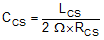
For instance, if RCS =1 mΩ, LCS = 1 nH, the required compensation capacitor CCS should be approximately 0.5 µF.
Note that selecting CCS greater than the value given by Equation 37 would over compensate the inductance and consequently defer the current zero crossing detection point to a negative current. Excessively larger capacitor should not be used to prevent malfunction of the controller.
 Figure 9-4 Effects of Parasitic Inductance on the Current Sense Signal and Zero Crossing Detection
 Figure 9-5 Compensation Network to Compensate the Current Sense Resistor’s Parasitic Inductance