ZHCSI27C April 2018 – October 2021 LM5036
PRODUCTION DATA
- 1 特性
- 2 应用
- 3 说明
- 4 Revision History
- 5 Pin Configuration and Functions
- 6 Specifications
-
7 Detailed Description
- 7.1 Overview
- 7.2 Functional Block Diagram
- 7.3
Feature Description
- 7.3.1 High-Voltage Start-Up Regulator
- 7.3.2 Undervoltage Lockout (UVLO)
- 7.3.3 Reference Regulator
- 7.3.4 Oscillator, Synchronized Input
- 7.3.5 Voltage-Mode Control
- 7.3.6 Primary-Side Gate Driver Outputs (LSG and HSG)
- 7.3.7 Half-Bridge PWM Scheme
- 7.3.8 Maximum Duty Cycle Operation
- 7.3.9 Pre-Biased Start-Up Process
- 7.3.10 Zero Duty Cycle Operation
- 7.3.11 Enhanced Cycle-by-Cycle Current Limiting with Pulse Matching
- 7.3.12 Reverse Current Protection
- 7.3.13 CBC Threshold Accuracy
- 7.3.14 Hiccup Mode Protection
- 7.3.15 Hiccup Mode Blanking
- 7.3.16 Over-Temperature Protection (OTP)
- 7.3.17 Over-Voltage / Latch (ON_OFF Pin)
- 7.3.18 Auxiliary Constant On-Time Control
- 7.3.19 Auxiliary On-Time Generator
- 7.3.20 Auxiliary Supply Current Limiting
- 7.3.21 Auxiliary Primary Output Capacitor Ripple
- 7.3.22 Auxiliary Ripple Configuration and Control
- 7.3.23 Asynchronous Mode Operation of Auxiliary Supply
- 7.4 Device Functional Modes
-
8 Application and Implementation
- 8.1 Application Information
- 8.2
Typical Application
- 8.2.1 Design Requirements
- 8.2.2
Detailed Design Procedure
- 8.2.2.1 Custom Design With WEBENCH® Tools
- 8.2.2.2 Input Transient Protection
- 8.2.2.3 Level-Shift Detection Circuit
- 8.2.2.4 Applications with VIN > 100-V
- 8.2.2.5 Applications without Pre-Biased Start-Up Requirement
- 8.2.2.6 UVLO Voltage Divider Selection
- 8.2.2.7 Over Voltage, Latch (ON_OFF Pin) Voltage Divider Selection
- 8.2.2.8 SS Capacitor
- 8.2.2.9 SSSR Capacitor
- 8.2.2.10 Half-Bridge Power Stage Design
- 8.2.2.11 Current Limit
- 8.2.2.12 Auxiliary Transformer
- 8.2.2.13 Auxiliary Feedback Resistors
- 8.2.2.14 RON Resistor
- 8.2.2.15 VIN Pin Capacitor
- 8.2.2.16 Auxiliary Primary Output Capacitor
- 8.2.2.17 Auxiliary Secondary Output Capacitor
- 8.2.2.18 Auxiliary Feedback Ripple Circuit
- 8.2.2.19 Auxiliary Secondary Diode
- 8.2.2.20 VCC Diode
- 8.2.2.21 Opto-Coupler Interface
- 8.2.2.22 Full-Bridge Converter Applications
- 8.2.3 Application Curves
- 9 Power Supply Recommendations
- 10Layout
- 11Device and Documentation Support
- 12Mechanical, Packaging, and Orderable Information
8.2.2.11 Current Limit
Section 7.3.11 describes the CBC current limiting functionality in detail. Figure 8-7 illustrates the current limiting block diagram of the LM5036 controller. These are the five resistors associated with the current limiting function of the half-bridge converter:
- RCS
- R3
- R2
- RLIM
- R1
Because R3 is equal to the equivalent resistance of R1 and R2 as given by Equation 13, there are four unknown resistor values to be determined.
 Figure 8-7 Current Limiting
Block
Figure 8-7 Current Limiting
BlockThe value of current sense resistor RCS is determined based on the maximum power consumption requirement. Typically, the current sense resistor should consume less than 0.5% of the input power of the converter at the worst case scenario. The sense resistor conducts every alternate current pulse flowing in the primary winding. The power dissipated in the sense resistor is determined by Equation 61.
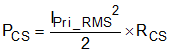
The RMS current flowing in the primary winding may be calculated using Equation 62.
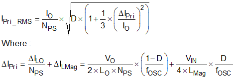
Maximum loss in the current sense resistor will occur while maximum output current (ILIM) is delivered from minimum input voltage (VIN(min)). Evaluating Equation 62 gives Equation 63.
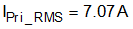
To achieve our target of dissipating less than 0.5% of maximum output power the current sense resistor must satisfy Equation 64.
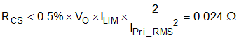
In our example design the current sense resistor value selected is given in Equation 65.

 Figure 8-8 Main Converter Operating
Waveforms
Figure 8-8 Main Converter Operating
WaveformsThe resistor R1 is used to set the slope compensation magnitude. In LM5036 device, the slope of the compensation ramp is given by Equation 66. To eliminate sub-harmonic oscillation, set mC to at least one-half the down-slope of output inductor current transformed to the primary side across the current sense resistor, as given by Equation 67 and Equation 68. To damp the sub-harmonic oscillation after one cycle, mC must be set equal to one times the down-slope of the output inductor current. This configuration is known as deadbeat control. In LM5036 controller, the slope compensation signal is a saw-tooth current waveform of magnitude ISLOPE at the oscillator frequency (twice the switching frequency).
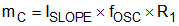
where
- mC is the slope of the compensation ramp
- ISLOPE is the amplitude of the saw-tooth current signal used for slope compensation
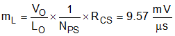
where
- mL is the down-slope of the output inductor current transformed to the primary side
- NP is the number of turns for the primary winding of the main transformer
- NS is the number of turns for the secondary winding of the main transformer
- VO is the output voltage of the half-bridge converter
- LO is the output inductor value of the half-bridge converter
- RCS is the current sense resistor value

Substituting Equation 66 and Equation 67 into Equation 68 gives an expression for the minimum value for resistor R1 to avoid sub-harmonic oscillation.
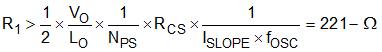
Doubling this value ensures deadbeat control. For this example design, the value given in Equation 70 are selected

Values have now been selected for both RCS and R1. Values for RLIM and R2 are yet to be determined. These values define the peak current limit threshold and how this level varies with input voltage. Equation 20, Equation 21 and Equation 25 define the relationship between peak primary current limit and maximum output current. For this design example ignore IBiasOffset and VCSOffset, because these parameters have only a small effect on output current limit. Setting these parameters to zero calculates Equation 71, Equation 72 and Equation 73.


The output current limit varies with input voltage. This design example limits the output current to ILIM at the extremes of input voltage giving Equation 74 and Equation 75. This value limits the spread of output current limit across the range of input voltage.
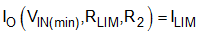
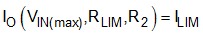
Solving Equation 74 and Equation 75 simultaneously yields values for resistors RLIM and R2.


Having determined values for R1 and R2, the value of resistor R3 is fixed by Equation 13.
The selected values for R2 and RLIM are given in Equation 78. Figure 8-9 presents the measured output current limit vs input voltage for the circuit presented in Figure 8-1. Figure 8-9 also presents the output current limit vs line for the same circuit predicted by Equation 71, Equation 72 and Equation 73. There is good agreement between measured and predicted results.
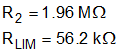
 Figure 8-9 Main Converter Measured vs
Predicted Output Current Limit
Figure 8-9 Main Converter Measured vs
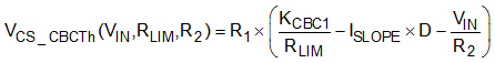
Predicted Output Current LimitIf the magnitude of the leading-edge spike is excessive, add an additional filter capacitor CF to form an RC filter with R1, to reduce the high-frequency noise spike. Both the leading-edge blanking (tCSBLK) and the RC filter help to prevent false triggering of the CBC current limiting operation.
The circuit connected to the CS_POS pin may be approximated by the simplified circuit shown in Figure 8-10.
 Figure 8-10 CS_POS Filter Circuit Model
and Waveform
Figure 8-10 CS_POS Filter Circuit Model
and WaveformThe voltage across the current sense resistor during the conduction period of the low-side MOSFET is represented by Equation 79.
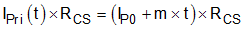
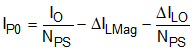
Where IP0 is the primary current at the start of the on period of the lower switch, and m is the slope of the primary current during the on period.
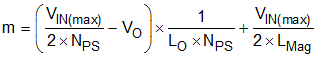
The voltage across capacitor CF for the circuit shown is expressed by Equation 82.
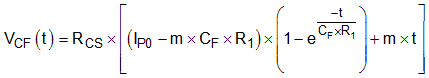
Let us assume that the on period of the lower switch is more than four times longer than the time constant made up of CF and R1. In this case the exponential term of Equation 82 tends to zero and the voltage across capacitor CF at the end of the tON period may be expressed by Equation 83.

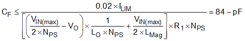
Comparing Equation 79 and Equation 83 shows that capacitor CF introduces an error in the sensed peak current given by Equation 84.
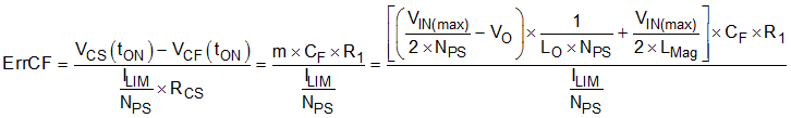
Hence, to ensure the error introduced by the filter capacitor is less than 2%, the value of capacitor CF should not exceed the value given by Equation 85.
The Excel Calculator Tool can be used to facilitate the process of calculating all the external CBC component values.