ZHCSI27C April 2018 – October 2021 LM5036
PRODUCTION DATA
- 1 特性
- 2 应用
- 3 说明
- 4 Revision History
- 5 Pin Configuration and Functions
- 6 Specifications
-
7 Detailed Description
- 7.1 Overview
- 7.2 Functional Block Diagram
- 7.3
Feature Description
- 7.3.1 High-Voltage Start-Up Regulator
- 7.3.2 Undervoltage Lockout (UVLO)
- 7.3.3 Reference Regulator
- 7.3.4 Oscillator, Synchronized Input
- 7.3.5 Voltage-Mode Control
- 7.3.6 Primary-Side Gate Driver Outputs (LSG and HSG)
- 7.3.7 Half-Bridge PWM Scheme
- 7.3.8 Maximum Duty Cycle Operation
- 7.3.9 Pre-Biased Start-Up Process
- 7.3.10 Zero Duty Cycle Operation
- 7.3.11 Enhanced Cycle-by-Cycle Current Limiting with Pulse Matching
- 7.3.12 Reverse Current Protection
- 7.3.13 CBC Threshold Accuracy
- 7.3.14 Hiccup Mode Protection
- 7.3.15 Hiccup Mode Blanking
- 7.3.16 Over-Temperature Protection (OTP)
- 7.3.17 Over-Voltage / Latch (ON_OFF Pin)
- 7.3.18 Auxiliary Constant On-Time Control
- 7.3.19 Auxiliary On-Time Generator
- 7.3.20 Auxiliary Supply Current Limiting
- 7.3.21 Auxiliary Primary Output Capacitor Ripple
- 7.3.22 Auxiliary Ripple Configuration and Control
- 7.3.23 Asynchronous Mode Operation of Auxiliary Supply
- 7.4 Device Functional Modes
-
8 Application and Implementation
- 8.1 Application Information
- 8.2
Typical Application
- 8.2.1 Design Requirements
- 8.2.2
Detailed Design Procedure
- 8.2.2.1 Custom Design With WEBENCH® Tools
- 8.2.2.2 Input Transient Protection
- 8.2.2.3 Level-Shift Detection Circuit
- 8.2.2.4 Applications with VIN > 100-V
- 8.2.2.5 Applications without Pre-Biased Start-Up Requirement
- 8.2.2.6 UVLO Voltage Divider Selection
- 8.2.2.7 Over Voltage, Latch (ON_OFF Pin) Voltage Divider Selection
- 8.2.2.8 SS Capacitor
- 8.2.2.9 SSSR Capacitor
- 8.2.2.10 Half-Bridge Power Stage Design
- 8.2.2.11 Current Limit
- 8.2.2.12 Auxiliary Transformer
- 8.2.2.13 Auxiliary Feedback Resistors
- 8.2.2.14 RON Resistor
- 8.2.2.15 VIN Pin Capacitor
- 8.2.2.16 Auxiliary Primary Output Capacitor
- 8.2.2.17 Auxiliary Secondary Output Capacitor
- 8.2.2.18 Auxiliary Feedback Ripple Circuit
- 8.2.2.19 Auxiliary Secondary Diode
- 8.2.2.20 VCC Diode
- 8.2.2.21 Opto-Coupler Interface
- 8.2.2.22 Full-Bridge Converter Applications
- 8.2.3 Application Curves
- 9 Power Supply Recommendations
- 10Layout
- 11Device and Documentation Support
- 12Mechanical, Packaging, and Orderable Information
7.3.18 Auxiliary Constant On-Time Control
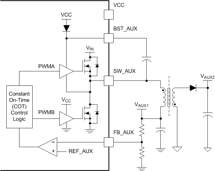
Figure 7-22 shows a block diagram of the constant on-time (COT) controlled fly-buck converter. The LM5036 device integrates an N-channel high-side MOSFET and associated high-voltage gate driver. The gate driver circuit works in conjunction with an external bootstrap capacitor and an internal high voltage diode. A 0.01-µF ceramic capacitor connected between the BST_AUX pin and SW_AUX pin provides the voltage to the driver during the on-time. During each off-time, the SW_AUX pin is at approximately 0-V, and the bootstrap capacitor charges from VCC through the internal diode. The minimum off-timer ensures a minimum time in each cycle to recharge the bootstrap capacitor. The LM5036 device also provides an internal N-channel SR MOSFET and associated driver. This MOSFET provides a path for the inductor current to flow when the high-side MOSFET is turned off.
The integrated auxiliary supply employs constant on-time (COT) hysteretic control which provides excellent transient response and ease of use. The control principle is based on a comparator and a one-shot on-timer, with the output voltage feedback (FB_AUX) compared to an internal reference. If the feedback voltage is below the reference the internal buck switch is switched on for the one-shot timer period, which is a function of the input voltage and the on-time resistor (RON). Following the on-time the switch remains off until the FB_AUX voltage falls below the reference, and the forced minimum off-time has expired. When the feedback voltage falls below the reference and the minimum off-time one-shot period expires, the high-side buck switch is then turned on for another on-time one-shot period. This will continue until regulation is achieved.
 Figure 7-22 COT Controlled Fly-Buck Auxiliary Supply Circuitry
In a fly-buck converter, the low-side SR MOSFET is on when the high-side switch is off. The inductor current ramps up when the high-side switch is on and ramps down when the low-side switch is on.
The switching frequency remains relatively constant with load and line variations. Use Equation 31 to calculate the switching frequency of the auxiliary supply.

where
- VAUX1 is the primary output voltage of the auxiliary supply.
Two external resistor values set the value of VAUX1. This regulation of the output voltage depends on ripple voltage at the feedback input, requiring a minimum amount of ESR for the output capacitor (CAUX1). A minimum of 25-mV of ripple voltage at the feedback pin is required for stable operation of the auxiliary supply. The Section 7.3.22 section describes auxiliary ripple circuit configuration.