ZHCSI27C April 2018 – October 2021 LM5036
PRODUCTION DATA
- 1 特性
- 2 应用
- 3 说明
- 4 Revision History
- 5 Pin Configuration and Functions
- 6 Specifications
-
7 Detailed Description
- 7.1 Overview
- 7.2 Functional Block Diagram
- 7.3
Feature Description
- 7.3.1 High-Voltage Start-Up Regulator
- 7.3.2 Undervoltage Lockout (UVLO)
- 7.3.3 Reference Regulator
- 7.3.4 Oscillator, Synchronized Input
- 7.3.5 Voltage-Mode Control
- 7.3.6 Primary-Side Gate Driver Outputs (LSG and HSG)
- 7.3.7 Half-Bridge PWM Scheme
- 7.3.8 Maximum Duty Cycle Operation
- 7.3.9 Pre-Biased Start-Up Process
- 7.3.10 Zero Duty Cycle Operation
- 7.3.11 Enhanced Cycle-by-Cycle Current Limiting with Pulse Matching
- 7.3.12 Reverse Current Protection
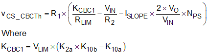
- 7.3.13 CBC Threshold Accuracy
- 7.3.14 Hiccup Mode Protection
- 7.3.15 Hiccup Mode Blanking
- 7.3.16 Over-Temperature Protection (OTP)
- 7.3.17 Over-Voltage / Latch (ON_OFF Pin)
- 7.3.18 Auxiliary Constant On-Time Control
- 7.3.19 Auxiliary On-Time Generator
- 7.3.20 Auxiliary Supply Current Limiting
- 7.3.21 Auxiliary Primary Output Capacitor Ripple
- 7.3.22 Auxiliary Ripple Configuration and Control
- 7.3.23 Asynchronous Mode Operation of Auxiliary Supply
- 7.4 Device Functional Modes
-
8 Application and Implementation
- 8.1 Application Information
- 8.2
Typical Application
- 8.2.1 Design Requirements
- 8.2.2
Detailed Design Procedure
- 8.2.2.1 Custom Design With WEBENCH® Tools
- 8.2.2.2 Input Transient Protection
- 8.2.2.3 Level-Shift Detection Circuit
- 8.2.2.4 Applications with VIN > 100-V
- 8.2.2.5 Applications without Pre-Biased Start-Up Requirement
- 8.2.2.6 UVLO Voltage Divider Selection
- 8.2.2.7 Over Voltage, Latch (ON_OFF Pin) Voltage Divider Selection
- 8.2.2.8 SS Capacitor
- 8.2.2.9 SSSR Capacitor
- 8.2.2.10 Half-Bridge Power Stage Design
- 8.2.2.11 Current Limit
- 8.2.2.12 Auxiliary Transformer
- 8.2.2.13 Auxiliary Feedback Resistors
- 8.2.2.14 RON Resistor
- 8.2.2.15 VIN Pin Capacitor
- 8.2.2.16 Auxiliary Primary Output Capacitor
- 8.2.2.17 Auxiliary Secondary Output Capacitor
- 8.2.2.18 Auxiliary Feedback Ripple Circuit
- 8.2.2.19 Auxiliary Secondary Diode
- 8.2.2.20 VCC Diode
- 8.2.2.21 Opto-Coupler Interface
- 8.2.2.22 Full-Bridge Converter Applications
- 8.2.3 Application Curves
- 9 Power Supply Recommendations
- 10Layout
- 11Device and Documentation Support
- 12Mechanical, Packaging, and Orderable Information
7.3.11 Enhanced Cycle-by-Cycle Current Limiting with Pulse Matching
Figure 7-11 illustrates the half-bridge converter with low-side current sensing using a sense resistor.
 Figure 7-11 Half-Bridge Converter with Low-Side Current Sensing
In LM5036 device, current limiting for the half-bridge converter is accomplished with three pins, including CS_SET, CS_POS and CS_ NEG pins, as shown in Figure 7-12. The current sense circuit limits positive current flowing from input to output and also negative current flowing from output to input. An input voltage compensation function helps to minimize the variation of effective output current limit across the range of input voltage. A pulse matching function is automatically implemented when the peak current limit circuit is active. This function matches the pulse width on the high and low primary FETs to maintain voltage balance of the half-bridge capacitor divider. This method ensures flux balance of the transformer during peak current limit operation.
 Figure 7-12 Block Diagram of the Current Limiting Function
CS_SET pin is used to set the internal current limit threshold with an external resistor RLIM according to Equation 7.

where
- VLIM (0.75-V typical) is the internal current limit setting voltage.
The CS_POS pin is driven by a signal representative of the current flowing through the low-side FET of the half-bridge converter. The current sense voltage at CS_POS pin (equal to CS_NEG pin voltage) is converted to a current sense signal through R3 which is then sensed, scaled and compared against the internal current limit thresholds. In order to blank the leading-edge transient noise seen when the low-side FET is turned on, the current sense signal is blanked for tCSBLK after LSG is turned on. If the magnitude of the noise spike is excessive, an additional filter capacitor CF may be added to form an RC filter with R1 to reduce the high-frequency noise spike. Both the leading-edge blanking and RC filter help to prevent false triggering of CBC current limiting operation.
In order to achieve bi-directional current sensing, an internal offset current (K10a x ICS_SET), is injected to the CS_POS pin. This offset allows positive internal thresholds on the CBC and NEG comparators that correspond to effective ICS_SET and -ICS_SET / 2 thresholds at the input.
When the current sense signal (IR3 x 1 / K10b) reaches the positive threshold (K2a x ICS_SET), CBC current limiting operation is activated. The controller essentially operates in peak current mode control, with the voltage loop open, during the CBC operation. A common issue with peak current mode control is sub-harmonic oscillation. This occurs when the effective duty cycle is greater than 50%. A common solution for sub-harmonic oscillation is to add slope compensation. The slope of the compensation ramp must be set to at least one half the downslope of the output inductor current transformed to the primary side across the current sense resistor. To eliminate sub-harmonic oscillation after one switching cycle, the slope compensation must be equal to the downslope of the output inductor current. This is known as deadbeat control. In LM5036, the slope compensation signal is a saw-tooth current signal ramping up from 0 to ISLOPE at the oscillator frequency (twice the switching frequency of each primary FET).
However, another issue will arise after slope compensation is added. The current limit level varies with the input voltage, as illustrated in Figure 7-13. Because the slope compensation magnitude is different at different input voltages, the actual current limit level varies with input voltage for a given internal current limit threshold.
 Figure 7-13 Current Sense and Current Limit Waveforms
A new feature, input voltage compensation, is provided by LM5036. By adding an extra signal, which is a function of input voltage, on top of the current sense signal and the slope compensation signal, variation of the current limit level can be minimized over the entire input voltage range. The CS_POS pin voltage at time t, after the rising edge of LSG, is expressed by Equation 8:

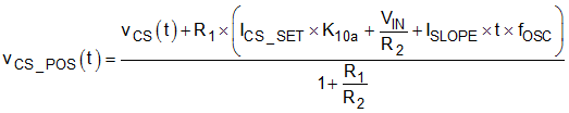
At the trip threshold, of the CBC comparator, both its inputs are at the same potential. In this case the voltage on the CS_NEG pin is expressed by Equation 10.
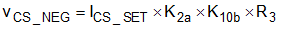
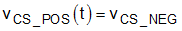
For a given duty cycle (D) the current sense threshold voltage that will just trigger the CBC comparator can be determined by combining Equation 9, Equation 10 and Equation 11.

Now if we assume:
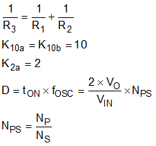
Equation 12 simplifies to Equation 14.
Section 8.2.2.11 gives an example design process for calculating the CBC external resistor values. The Excel Calculator Tool can also be used to assist in the process of selecting these resistor values.
LM5036 ensures flux balance of the main transformer during CBC operation. The duty cycles of the two primary FETs are always matched. If the low-side FET is terminated due to a current limit event, a matched duty cycle will be applied to the high-side FET during the next half switching period, regardless of the current condition. The matched duty cycles ensure voltage-second balance of the transformer which prevents transformer saturation.
The pulse matching operation is illustrated in Figure 7-14. When the current limit is reached during the low-side phase, a FLAG signal goes high. The RAMP signal is sampled at the rising edge of the FLAG signal and then held through the next half switching period for the high-side phase. When the high-side phase RAMP signal rises above the sampled value, the high-side PWM pulse is turned off so that the duty cycle are matched for both phases. In the meantime, the hiccup restart capacitor is charged with a current source IRES-SRC1 (15-µA typical) during CBC operation. The pulse matching feature is handled automatically by the LM5036 controller and requires no action from the designer.
 Figure 7-14 Pulse Matching Operation