ZHCSI27C April 2018 – October 2021 LM5036
PRODUCTION DATA
- 1 特性
- 2 应用
- 3 说明
- 4 Revision History
- 5 Pin Configuration and Functions
- 6 Specifications
-
7 Detailed Description
- 7.1 Overview
- 7.2 Functional Block Diagram
- 7.3
Feature Description
- 7.3.1 High-Voltage Start-Up Regulator
- 7.3.2 Undervoltage Lockout (UVLO)
- 7.3.3 Reference Regulator
- 7.3.4 Oscillator, Synchronized Input
- 7.3.5 Voltage-Mode Control
- 7.3.6 Primary-Side Gate Driver Outputs (LSG and HSG)
- 7.3.7 Half-Bridge PWM Scheme
- 7.3.8 Maximum Duty Cycle Operation
- 7.3.9 Pre-Biased Start-Up Process
- 7.3.10 Zero Duty Cycle Operation
- 7.3.11 Enhanced Cycle-by-Cycle Current Limiting with Pulse Matching
- 7.3.12 Reverse Current Protection
- 7.3.13 CBC Threshold Accuracy
- 7.3.14 Hiccup Mode Protection
- 7.3.15 Hiccup Mode Blanking
- 7.3.16 Over-Temperature Protection (OTP)
- 7.3.17 Over-Voltage / Latch (ON_OFF Pin)
- 7.3.18 Auxiliary Constant On-Time Control
- 7.3.19 Auxiliary On-Time Generator
- 7.3.20 Auxiliary Supply Current Limiting
- 7.3.21 Auxiliary Primary Output Capacitor Ripple
- 7.3.22 Auxiliary Ripple Configuration and Control
- 7.3.23 Asynchronous Mode Operation of Auxiliary Supply
- 7.4 Device Functional Modes
-
8 Application and Implementation
- 8.1 Application Information
- 8.2
Typical Application
- 8.2.1 Design Requirements
- 8.2.2
Detailed Design Procedure
- 8.2.2.1 Custom Design With WEBENCH® Tools
- 8.2.2.2 Input Transient Protection
- 8.2.2.3 Level-Shift Detection Circuit
- 8.2.2.4 Applications with VIN > 100-V
- 8.2.2.5 Applications without Pre-Biased Start-Up Requirement
- 8.2.2.6 UVLO Voltage Divider Selection
- 8.2.2.7 Over Voltage, Latch (ON_OFF Pin) Voltage Divider Selection
- 8.2.2.8 SS Capacitor
- 8.2.2.9 SSSR Capacitor
- 8.2.2.10 Half-Bridge Power Stage Design
- 8.2.2.11 Current Limit
- 8.2.2.12 Auxiliary Transformer
- 8.2.2.13 Auxiliary Feedback Resistors
- 8.2.2.14 RON Resistor
- 8.2.2.15 VIN Pin Capacitor
- 8.2.2.16 Auxiliary Primary Output Capacitor
- 8.2.2.17 Auxiliary Secondary Output Capacitor
- 8.2.2.18 Auxiliary Feedback Ripple Circuit
- 8.2.2.19 Auxiliary Secondary Diode
- 8.2.2.20 VCC Diode
- 8.2.2.21 Opto-Coupler Interface
- 8.2.2.22 Full-Bridge Converter Applications
- 8.2.3 Application Curves
- 9 Power Supply Recommendations
- 10Layout
- 11Device and Documentation Support
- 12Mechanical, Packaging, and Orderable Information
7.3.20 Auxiliary Supply Current Limiting
The LM5036 controller contains an intelligent current limit off-timer for the auxiliary supply. If the current in the high-side switch exceeds IAUX(LIM) (200-mA typical), both the high-side MOSFET and the low-side SR are immediately turned off, and a non-resetable off-timer is initiated. The length of the off-time is a function of the FB_AUX pin voltage and the input voltage VIN. As an example, when VFB_AUX = 0 V and VIN = 48 V, a maximum off-time is set to 16 µs. This condition occurs when the output is shorted, and during the initial phase of start-up. This amount of time ensures safe short-circuit operation up to the maximum input voltage of 100 V.
In cases of overload where the FB_AUX voltage is above zero volts (not a short circuit) the current limit off-time is reduced. Reducing the off-time during less severe overloads reduces the amount of foldback, recovery time, and start-up time. The current limit off-time is calculated from Equation 33.

Because the current limit protection feature of the auxiliary supply is peak limited, the maximum average output is less than the peak.
To prevent excessive reverse current during the off-time of the current limit, the auxiliary supply operates in asynchronous (ASYNC) mode where the low-side SR is turned off during current limit operation. The body diode of the internal low-side MOSFET (QB) incurs significant power loss during asynchronous operation. TI recommends adding an external schottky diode (DFW) between the PGND and SW_AUX pins to ensure robust and efficient current limit operation. This schottky diode is particularly important when operating from high input voltage. Use an external schottky diode (DFW) that is rated to carry the maximum auxiliary current and block the maximum input voltage (VIN(max)).
For high density designs it is desirable to use an auxiliary transformer with low magnetising inductance and saturation current. The peak magnetising current flowing in the auxiliary transformer can exceed IAUX(LIM) due to delays in the peak current detection and comparator circuit. The actual peak magnetising current reached is a function of the maximum slope of the transformer magnetising current. This behavior depends upon both maximum input voltage VIN(max) and magnetising inductance value. The method outlined below allows designers to estimate the peak magnetising current that will flow in the Aux transformer (ILPk).
As illustrated in Figure 7-25, it is convenient to model the internal current sense circuit as a simple RC time constant, τAuxSns (41-ns typical), that delays the sensed current signal presented to the OCP comparator input. There is a further delay tAUX(LIM) (116-ns typical), after the comparator input reaches its trip threshold before the OCPb fault flag is set. The controller applies this extended off time, tOFF(ILIM), only if the OCPb fault flag is set before the COT (tON) period ends. Equation 34 is an expression for the sensed and delayed magnetising current inductor signal applied to the non-inverting input of the OCP comparator.
 Figure 7-25 Aux Current Limit Circuit Model
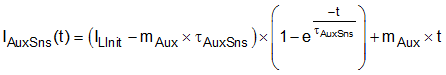
where
- mAux is the slope of Aux transformer magnetising inductor current during QA on period
- τAuxSns is the time constant of the internal current sensing circuit feeding the OCP comparator
Maximum peak current occurs when the magnetising inductor current slope has its highest value. This peak occurs at start-up, or when a short circuit is applied across the VAUX1 output, while operating from maximum input voltage (VIN(max)). The maximum inductor current slope is given by Equation 35.
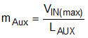
where
- LAUX is the magnetising inductance of the Aux transformer
For a use case where the inductor current slope is fixed at its maximum value (mAux), the highest peak current occurs when the inductor current at the start of the pulse (ILInit) is just high enough to trip the OCPb flag before the COT period (tON) expires. After this trip occurrs, the controller applies the extended OFF period (tOFF(ILIM)) to reduce the inductor current for subsequent pulses. This condition is given in Equation 36 and is shown graphically in Figure 7-25

where
- tAUX(LIM) is the time delay between comparator input threshold being achieved and the OCPb flag set
Combining Equation 34 and Equation 36 determines the initial inductor current for a pulse containing the highest peak current Equation 37.
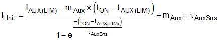
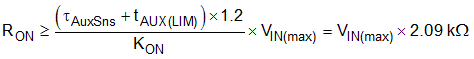
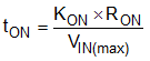
Equation 38 uses the COT period in Equation 37 for the maximum input voltage.
where
- KON (9 × 10–11 typical) is an internal constant that defines the COT period for a given VIN and RON
Having calculated ILInit the estimated peak inductor current is given by Equation 39.

Use this method to ensure that the operation does not exceed the Aux transformer saturation current under transient or fault conditions. This method assumes fixed transformer magnetising inductance. The method provides only a reasonable accuracy if the transformer magnetising inductance has not fallen significantly at the predicted peak current.
To avoid excessive peak magnetising current during transient or fault events, ensure that the COT period (tON) is longer than the response time of the peak current protection circuit. Equation 40 expresses it as a minimum required value for RON .