ZHCSI27C April 2018 – October 2021 LM5036
PRODUCTION DATA
- 1 特性
- 2 应用
- 3 说明
- 4 Revision History
- 5 Pin Configuration and Functions
- 6 Specifications
-
7 Detailed Description
- 7.1 Overview
- 7.2 Functional Block Diagram
- 7.3
Feature Description
- 7.3.1 High-Voltage Start-Up Regulator
- 7.3.2 Undervoltage Lockout (UVLO)
- 7.3.3 Reference Regulator
- 7.3.4 Oscillator, Synchronized Input
- 7.3.5 Voltage-Mode Control
- 7.3.6 Primary-Side Gate Driver Outputs (LSG and HSG)
- 7.3.7 Half-Bridge PWM Scheme
- 7.3.8 Maximum Duty Cycle Operation
- 7.3.9 Pre-Biased Start-Up Process
- 7.3.10 Zero Duty Cycle Operation
- 7.3.11 Enhanced Cycle-by-Cycle Current Limiting with Pulse Matching
- 7.3.12 Reverse Current Protection
- 7.3.13 CBC Threshold Accuracy
- 7.3.14 Hiccup Mode Protection
- 7.3.15 Hiccup Mode Blanking
- 7.3.16 Over-Temperature Protection (OTP)
- 7.3.17 Over-Voltage / Latch (ON_OFF Pin)
- 7.3.18 Auxiliary Constant On-Time Control
- 7.3.19 Auxiliary On-Time Generator
- 7.3.20 Auxiliary Supply Current Limiting
- 7.3.21 Auxiliary Primary Output Capacitor Ripple
- 7.3.22 Auxiliary Ripple Configuration and Control
- 7.3.23 Asynchronous Mode Operation of Auxiliary Supply
- 7.4 Device Functional Modes
-
8 Application and Implementation
- 8.1 Application Information
- 8.2
Typical Application
- 8.2.1 Design Requirements
- 8.2.2
Detailed Design Procedure
- 8.2.2.1 Custom Design With WEBENCH® Tools
- 8.2.2.2 Input Transient Protection
- 8.2.2.3 Level-Shift Detection Circuit
- 8.2.2.4 Applications with VIN > 100-V
- 8.2.2.5 Applications without Pre-Biased Start-Up Requirement
- 8.2.2.6 UVLO Voltage Divider Selection
- 8.2.2.7 Over Voltage, Latch (ON_OFF Pin) Voltage Divider Selection
- 8.2.2.8 SS Capacitor
- 8.2.2.9 SSSR Capacitor
- 8.2.2.10 Half-Bridge Power Stage Design
- 8.2.2.11 Current Limit
- 8.2.2.12 Auxiliary Transformer
- 8.2.2.13 Auxiliary Feedback Resistors
- 8.2.2.14 RON Resistor
- 8.2.2.15 VIN Pin Capacitor
- 8.2.2.16 Auxiliary Primary Output Capacitor
- 8.2.2.17 Auxiliary Secondary Output Capacitor
- 8.2.2.18 Auxiliary Feedback Ripple Circuit
- 8.2.2.19 Auxiliary Secondary Diode
- 8.2.2.20 VCC Diode
- 8.2.2.21 Opto-Coupler Interface
- 8.2.2.22 Full-Bridge Converter Applications
- 8.2.3 Application Curves
- 9 Power Supply Recommendations
- 10Layout
- 11Device and Documentation Support
- 12Mechanical, Packaging, and Orderable Information
7.3.22 Auxiliary Ripple Configuration and Control
The voltage ripple across the output capacitor CAUX1 is made up of two components:
- Resistive ripple appears across the equivalent series resistance (ESR) of the output capacitor. This component of ripple is in phase with the inductor current and is 90° delayed compared with the applied PWM signal.
- Capacitive ripple appears across the ideal capacitor. This component of ripple is 90° delayed compared with the inductor current ripple and 180° delayed compared with the applied PWM signal.
With COT control, the on-time of the high-side FET is terminated by an on-timer, and the off-time is terminated when the feedback voltage VFB_AUX falls below the reference voltage (VAUX-ON). For a buck topology this type of hysteretic control provides stable operation if these two conditions are met:
- Output voltage ripple is dominated by the resistive ESR component. The resistive ripple amplitude must be approximately five times the capacitive ripple amplitude to guarantee stable operation.
- Output voltage ripple amplitude present at the FB_AUX pin must be greater than noise coupled onto this pin from other sources. For an output voltage ripple amplitude of 25 mV at the FB_AUX pin ensures that other sources of noise coupled to the pin can be assumed small
Aux transformer magnetising inductor ripple current amplitude is expressed by Equation 43.
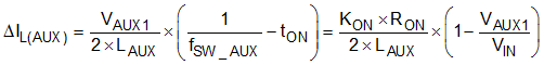
For a buck converter the capacitive component of output voltage ripple amplitude is expressed by Equation 92. The resistive component of output ripple voltage amplitude is expressed by Equation 44.
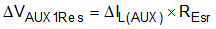
Our condition for stable operation requires that Equation 45 and Equation 46 are both satisfied.


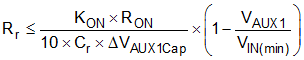
The method outlined above allows us to calculate the resistance (REsr) that must be present in series with the output capacitor (CAUX1) to provide stable operation of a buck converter. This simple method has disadvantages of high output voltage ripple amplitude and high dissipation in the series resistor REsr. The method is also not ideal for a flybuck topology, especially if most of the load current is drawn from the secondary winding. In this case much of the magnetising inductor current flows into the secondary output capacitor (CAUX2) and not the primary output capacitor (CAUX1) during the low-side FET conduction period (tOFF). The circuit of Figure 7-27 provides a better solution that is well suited to the flybuck topology. A series branch Rr – Cr is connected across LAUX. The controller applies the same PWM voltage across this series branch as appears across LAUX. Assuming most of the PWM voltage is dropped across Rr, the voltage across Cr has the almost the same shape and phase as the inductor current. The voltage ripple across Cr can be used to substitute the voltage across RESR and thus provide stable operation without the need for high output ripple and dissipation. By coupling this capacitor voltage signal directly to the FB_AUX pin we can achieve the same result as a large ESR resistor, but without the penalty of dissipation and high output voltage ripple amplitude. The method is suitable for a flybuck topology, since the down-slope of the magnetising current is synthesised, across Cr, and therefore available on the primary side to couple onto the FB_AUX pin.
 Figure 7-27 Minimum Ripple
Configuration
Figure 7-27 Minimum Ripple
ConfigurationThe impedance of the capacitor generating the synthesised inductor current ripple signal, at the Aux switching frequency (fSW_AUX), must be low compared with the impedance of the RFBx divider network.
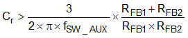
The synthesised inductor ripple, generated across Cr, is added to the ripple across the output capacitor (CAUX1). The resultant signal is coupled to the FB_AUX pin via capacitor Cac. The value of series resistor Rr is chosen to ensure the synthesised resistive ripple amplitude satisfies Equation 45 giving Equation 48.
Capacitor Cac couples the ripple signal directly onto the FB_AUX pin. Ensure that the value of this capacitor is at least five times greater than the value of Cr. This ratio ensures minimum attenuation and phase shift of the coupled ripple signal.
