ZHCSI27C April 2018 – October 2021 LM5036
PRODUCTION DATA
- 1 特性
- 2 应用
- 3 说明
- 4 Revision History
- 5 Pin Configuration and Functions
- 6 Specifications
-
7 Detailed Description
- 7.1 Overview
- 7.2 Functional Block Diagram
- 7.3
Feature Description
- 7.3.1 High-Voltage Start-Up Regulator
- 7.3.2 Undervoltage Lockout (UVLO)
- 7.3.3 Reference Regulator
- 7.3.4 Oscillator, Synchronized Input
- 7.3.5 Voltage-Mode Control
- 7.3.6 Primary-Side Gate Driver Outputs (LSG and HSG)
- 7.3.7 Half-Bridge PWM Scheme
- 7.3.8 Maximum Duty Cycle Operation
- 7.3.9 Pre-Biased Start-Up Process
- 7.3.10 Zero Duty Cycle Operation
- 7.3.11 Enhanced Cycle-by-Cycle Current Limiting with Pulse Matching
- 7.3.12 Reverse Current Protection
- 7.3.13 CBC Threshold Accuracy
- 7.3.14 Hiccup Mode Protection
- 7.3.15 Hiccup Mode Blanking
- 7.3.16 Over-Temperature Protection (OTP)
- 7.3.17 Over-Voltage / Latch (ON_OFF Pin)
- 7.3.18 Auxiliary Constant On-Time Control
- 7.3.19 Auxiliary On-Time Generator
- 7.3.20 Auxiliary Supply Current Limiting
- 7.3.21 Auxiliary Primary Output Capacitor Ripple
- 7.3.22 Auxiliary Ripple Configuration and Control
- 7.3.23 Asynchronous Mode Operation of Auxiliary Supply
- 7.4 Device Functional Modes
-
8 Application and Implementation
- 8.1 Application Information
- 8.2
Typical Application
- 8.2.1 Design Requirements
- 8.2.2
Detailed Design Procedure
- 8.2.2.1 Custom Design With WEBENCH® Tools
- 8.2.2.2 Input Transient Protection
- 8.2.2.3 Level-Shift Detection Circuit
- 8.2.2.4 Applications with VIN > 100-V
- 8.2.2.5 Applications without Pre-Biased Start-Up Requirement
- 8.2.2.6 UVLO Voltage Divider Selection
- 8.2.2.7 Over Voltage, Latch (ON_OFF Pin) Voltage Divider Selection
- 8.2.2.8 SS Capacitor
- 8.2.2.9 SSSR Capacitor
- 8.2.2.10 Half-Bridge Power Stage Design
- 8.2.2.11 Current Limit
- 8.2.2.12 Auxiliary Transformer
- 8.2.2.13 Auxiliary Feedback Resistors
- 8.2.2.14 RON Resistor
- 8.2.2.15 VIN Pin Capacitor
- 8.2.2.16 Auxiliary Primary Output Capacitor
- 8.2.2.17 Auxiliary Secondary Output Capacitor
- 8.2.2.18 Auxiliary Feedback Ripple Circuit
- 8.2.2.19 Auxiliary Secondary Diode
- 8.2.2.20 VCC Diode
- 8.2.2.21 Opto-Coupler Interface
- 8.2.2.22 Full-Bridge Converter Applications
- 8.2.3 Application Curves
- 9 Power Supply Recommendations
- 10Layout
- 11Device and Documentation Support
- 12Mechanical, Packaging, and Orderable Information
7.3.12 Reverse Current Protection
In addition to the CBC current limit, a negative current limit, which is set to be half of the positive current limit as shown in Figure 7-15. This is used to prevent excessive reverse current which could cause significant output voltage dip and potentially damage the power converter. When the negative current limit is exceeded twice, the SSSR capacitor will be clamped to ground so the controller enters the SR SYNC mode where the SR pulses are synchronized to the respective primary FET pulses. Therefore, the SR freewheeling pulses are turned off. The negative current limit event counter will be reset if the number of negative current limit events detected within four switching periods is less than two.
 Figure 7-15 Reverse Current Protection Circuit
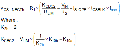
At the trip threshold of the NEG comparator both inputs are at the same potential. In this case the voltage on the CS_NEG pin is expressed by Equation 15.
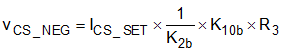
The voltage across the CS resistor at the trip threshold of the NEG comparator can therefore be determined by combining Equation 9, Equation 11 and Equation 15.
Notice that the inductor current has its most negative value at the start of the LSG on period. The NEG comparator trip will occur immediately after the blanking period (tCSBLK) has expired.
The Excel Calculator Tool predicts both the positive and negative output current limit levels as a function of input voltage for a given set of resistor values.