ZHCSDG6C March 2015 – January 2023 DRV2700
PRODUCTION DATA
- 1 特性
- 2 应用
- 3 说明
- 4 Revision History
- 5 Pin Configuration and Functions
- 6 Specifications
- 7 Detailed Description
-
8 Application and Implementation
- 8.1 Application Information
- 8.2
Typical Applications
- 8.2.1
AC-Coupled DAC Input Application
- 8.2.1.1 Design Requirements
- 8.2.1.2
Detailed Design Procedure
- 8.2.1.2.1 Piezo Load Selection
- 8.2.1.2.2 Programming The Boost Voltage
- 8.2.1.2.3 Inductor and Transformer Selection
- 8.2.1.2.4 Programing the Boost and Flyback Current-Limit
- 8.2.1.2.5 Boost Capacitor Selection
- 8.2.1.2.6 Pulldown FET and Resistors
- 8.2.1.2.7 Low-Voltage Operation
- 8.2.1.2.8 Current Consumption Calculation
- 8.2.1.2.9 Input Filter Considerations
- 8.2.1.2.10 Output Limiting Factors
- 8.2.1.2.11 Startup and Shutdown Sequencing
- 8.2.1.3 Application Curves
- 8.2.2 Filtered AC Coupled Single-Ended PWM Input Application
- 8.2.3 DC-Coupled DAC Input Application
- 8.2.4 DC-Coupled Reference Input Application
- 8.2.5 Flyback Circuit
- 8.2.1
AC-Coupled DAC Input Application
- 8.3 System Example
- 9 Power Supply Recommendations
- 10Layout
- 11Device and Documentation Support
- 12Mechanical, Packaging, and Orderable Information
封装选项
请参考 PDF 数据表获取器件具体的封装图。
机械数据 (封装 | 引脚)
- RGP|20
散热焊盘机械数据 (封装 | 引脚)
- RGP|20
订购信息
8.2.4 DC-Coupled Reference Input Application
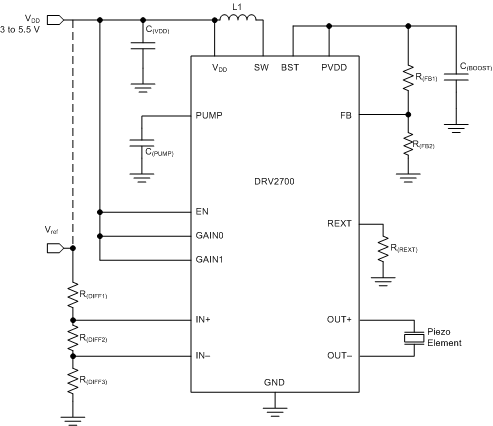
The DC-coupled referenced to VDD input is used in applications when the user might need to drive the output at a constant DC level in an on-off implementation. A typical application for this configuration is for piezo pneumatic valves. A benefit to this application circuit is that all of the inputs, including power, are at a very low voltage while keeping the high-voltage piezo load separated. Additionally, all that is required is the VDD input. This feature allows easy implementation into systems and to help separate or isolate the high voltages loads from the critical controls.
As mentioned in the previous section, piezoelectric materials have a certain voltage that debias the piezo phenomenon. This configuration protects the piezo from negative voltages because the input is always positive.
 Figure 8-14 DC-Coupled Referenced Input
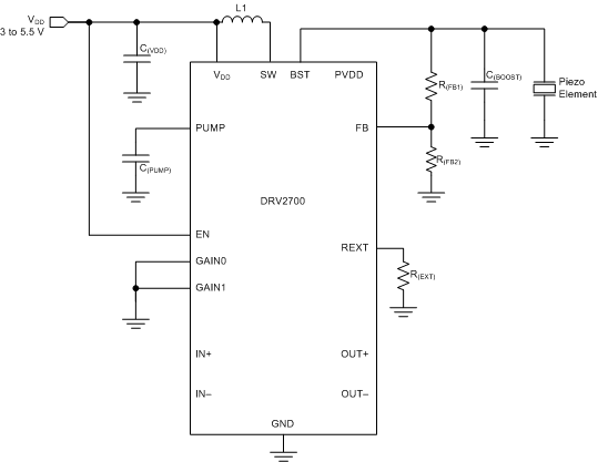
This application circuit can also be altered to only use the boost as shown in Figure 8-15. The benefits of altering this circuit is that it requires less components and has better power efficiency because no power is used in the amplifier. The drawback is that ripple occurs on the piezo element and the fall time of the output is longer because it is drained based on the RC time constant on the BST node.
 Figure 8-15 Boost Driving Piezo