ZHCSDG6C March 2015 – January 2023 DRV2700
PRODUCTION DATA
- 1 特性
- 2 应用
- 3 说明
- 4 Revision History
- 5 Pin Configuration and Functions
- 6 Specifications
- 7 Detailed Description
-
8 Application and Implementation
- 8.1 Application Information
- 8.2
Typical Applications
- 8.2.1
AC-Coupled DAC Input Application
- 8.2.1.1 Design Requirements
- 8.2.1.2
Detailed Design Procedure
- 8.2.1.2.1 Piezo Load Selection
- 8.2.1.2.2 Programming The Boost Voltage
- 8.2.1.2.3 Inductor and Transformer Selection
- 8.2.1.2.4 Programing the Boost and Flyback Current-Limit
- 8.2.1.2.5 Boost Capacitor Selection
- 8.2.1.2.6 Pulldown FET and Resistors
- 8.2.1.2.7 Low-Voltage Operation
- 8.2.1.2.8 Current Consumption Calculation
- 8.2.1.2.9 Input Filter Considerations
- 8.2.1.2.10 Output Limiting Factors
- 8.2.1.2.11 Startup and Shutdown Sequencing
- 8.2.1.3 Application Curves
- 8.2.2 Filtered AC Coupled Single-Ended PWM Input Application
- 8.2.3 DC-Coupled DAC Input Application
- 8.2.4 DC-Coupled Reference Input Application
- 8.2.5 Flyback Circuit
- 8.2.1
AC-Coupled DAC Input Application
- 8.3 System Example
- 9 Power Supply Recommendations
- 10Layout
- 11Device and Documentation Support
- 12Mechanical, Packaging, and Orderable Information
封装选项
请参考 PDF 数据表获取器件具体的封装图。
机械数据 (封装 | 引脚)
- RGP|20
散热焊盘机械数据 (封装 | 引脚)
- RGP|20
订购信息
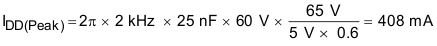
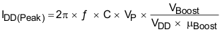
8.2.1.2.8 Current Consumption Calculation
Understanding how the voltage driven onto a piezo actuator relates to the current consumption from the power supply is useful. Modeling a piezo element as a pure capacitor is reasonably accurate. Use Equation 4 to calculate the current through a capacitor for an applied sinusoid.

- ƒ is the frequency of the sinusoid in hertz
- C is the capacitance of the piezo load in farads
- VP is the peak voltage
At the power supply, the actuator current is multiplied by the boost-supply ratio and divided by the efficiency of the boost converter as shown in Equation 5.
Substituting the design example values for the variables into Equation 5 and using a boost efficiency of 60%, yields a typical peak current from the power supply of 408 mA as shown in Equation 6.