ZHCSDG6C March 2015 – January 2023 DRV2700
PRODUCTION DATA
- 1 特性
- 2 应用
- 3 说明
- 4 Revision History
- 5 Pin Configuration and Functions
- 6 Specifications
- 7 Detailed Description
-
8 Application and Implementation
- 8.1 Application Information
- 8.2
Typical Applications
- 8.2.1
AC-Coupled DAC Input Application
- 8.2.1.1 Design Requirements
- 8.2.1.2
Detailed Design Procedure
- 8.2.1.2.1 Piezo Load Selection
- 8.2.1.2.2 Programming The Boost Voltage
- 8.2.1.2.3 Inductor and Transformer Selection
- 8.2.1.2.4 Programing the Boost and Flyback Current-Limit
- 8.2.1.2.5 Boost Capacitor Selection
- 8.2.1.2.6 Pulldown FET and Resistors
- 8.2.1.2.7 Low-Voltage Operation
- 8.2.1.2.8 Current Consumption Calculation
- 8.2.1.2.9 Input Filter Considerations
- 8.2.1.2.10 Output Limiting Factors
- 8.2.1.2.11 Startup and Shutdown Sequencing
- 8.2.1.3 Application Curves
- 8.2.2 Filtered AC Coupled Single-Ended PWM Input Application
- 8.2.3 DC-Coupled DAC Input Application
- 8.2.4 DC-Coupled Reference Input Application
- 8.2.5 Flyback Circuit
- 8.2.1
AC-Coupled DAC Input Application
- 8.3 System Example
- 9 Power Supply Recommendations
- 10Layout
- 11Device and Documentation Support
- 12Mechanical, Packaging, and Orderable Information
封装选项
请参考 PDF 数据表获取器件具体的封装图。
机械数据 (封装 | 引脚)
- RGP|20
散热焊盘机械数据 (封装 | 引脚)
- RGP|20
订购信息
8.2.5 Flyback Circuit
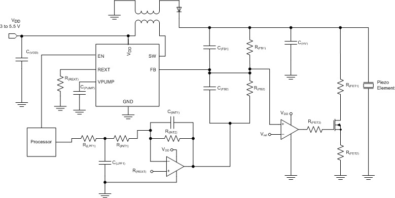
The flyback circuit is intended for applications using piezo valves, piezo polymers, and other high-voltage loads. The previously listed applications go from ±100 V, however this circuit can go up to even higher voltages (1 kV for example) depending on the feedback network and maximum operating conditions of the external components. The input is controlled using PWM, a DAC, or a purely analog signal. Therefore, a proper input filter may be required as discussed in the previous application circuits.
The increased voltage range, however, comes at a price. As the output voltage increases, the capable output sourcing current is lowered. However, because most piezo loads require a small current for the holding or blocking force, the drop in current may not impact the performance of the application. Figure 8-16 shows a typical flyback circuit.
 Figure 8-16 Flyback Circuit
The following sections shown in Figure 8-16 must be explained:
- Op-amp integrator
- Comparator and pulldown FET
- C(HV) value
The op-amp integrator shown at the bottom of the circuit in Figure 8-16, is used to control the output voltage. Because the input can be a PWM or DAC signal, it helps smooth out the input signal. Additionally, the output controls the virtual ground of the feedback network. For example, when the output of the integrator is equal to VOL (approximately 0 V), the current through R(FB2) is at the maximum and therefore increase the current (and voltage) on R(FB1) which raises the voltage across the piezo load. Likewise, as the output voltage of the integrator increases, it then decreases the current through R(FB2) and therefore decreases the voltage on R(FB1), which lowers the voltage across the piezo load.
The comparator and pulldown FET are used to drain the charge on the high-voltage output. Because a high resistance (or low current) is desired through for the feedback network, the RC-time constant of draining charge can be very long. To help with this long RC-time constraint, the comparator and pulldown FET are added to drain charge when VFB > Vref which adds a low resistance in parallel and therefore lowers the RC time constant. Ensure that this pulldown network can support the voltage and the current. As shown in Figure 8-9 and Figure 8-10, the pulldown allows for better regulation and faster stopping time.
Lastly, the C(HV) value is determined by the system. A value of >1-nF total capacitance is required on the high-voltage node for proper regulation. This total capacitance is the combination of the piezo load and the onboard C(HV).
As the capacitance increases, the voltage ripple on the output decreases. However, this decrease in ripple also slows down the startup or slew rate on the output. Ensure that the C(HV) and the piezo load can support the high voltage across C(HV) and the load.