ZHCSO15A December 2021 – February 2023 DLPC4420
PRODUCTION DATA
- 1 特性
- 2 应用
- 3 说明
- 4 Revision History
- 5 Pin Configuration and Functions
-
6 Specifications
- 6.1 Absolute Maximum Ratings
- 6.2 ESD Ratings
- 6.3 Recommended Operating Conditions
- 6.4 Thermal Information
- 6.5 Electrical Characteristics
- 6.6 System Oscillators Timing Requirements
- 6.7 Test and Reset Timing Requirements
- 6.8 JTAG Interface: I/O Boundary Scan Application Timing Requirements
- 6.9 Port 1 Input Pixel Timing Requirements
- 6.10 Port 3 Input Pixel Interface (via GPIO) Timing Requirements
- 6.11 DMD LVDS Interface Timing Requirements
- 6.12 Synchronous Serial Port (SSP) Interface Timing Requirements
- 6.13 Programmable Output Clocks Switching Characteristics
- 6.14 Synchronous Serial Port Interface (SSP) Switching Characteristics
- 6.15 JTAG Interface: I/O Boundary Scan Application Switching Characteristics
-
7 Detailed Description
- 7.1 Overview
- 7.2 Functional Block Diagram
- 7.3 Feature Description
- 7.4 Device Functional Modes
- 8 Application and Implementation
- 9 Power Supply Recommendations
- 10Layout
- 11Device and Documentation Support
- 12Mechanical, Packaging, and Orderable Information
10.1.1 PCB Layout Guidelines for Internal DLPC4420 Power
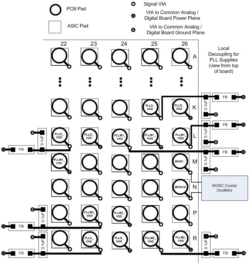
The following guidelines to achieve desired controller performance relative to internal PLLs are recommended:
- The DLPC4420 controller contains four PLLs (PLLM1, PLLM2, PLLD and PLLS), each of which have a dedicated 1.1V digital supply, and three (PLLM1, PLLM2 and PLLD) which have a dedicated 1.8-V analog supply. It is important to have filtering on the supply pins that covers a broad frequency range. Each 1.1V PLL supply pin must have individual high frequency filtering in the form of a ferrite bead and a 0.1µF ceramic capacitor. These components must be located very close to the individual PLL supply balls. The impedance of the ferrite bead must be greater than that of the capacitor at frequencies above 10MHz. The 1.1V to the PLL supply pins must also have low frequency filtering in the form of an RC filter. This filter can be common to all the PLLs. The voltage drop across the resistor is limited by the 1.1V regulator tolerance and the DLPC4420 device voltage tolerance. A resistance of 0.36 Ω and a 100 µF ceramic are recommended.
- The analog 1.8V PLL power pins must have a similar filter topology as the 1.1V. In addition, it is recommended that the 1.8V be generated with a dedicated linear regulator.
- When designing the overall supply filter network, care must be taken to ensure no resonance occurs. Particular care must be taken around the 1 to 2MHz band, as this coincides with the PLL natural loop frequency.
 Figure 10-1 PLL Filter Layout
High frequency decoupling is required for both 1.1V and 1.8V PLL supplies and must be provided as close as possible to each of the PLL supply package pins. It is recommended to place decoupling capacitors under the package on the opposite side of the board. Use high quality, low-ESR, monolithic, surface mount capacitors. Typically 0.1µF for each PLL supply is sufficient. The length of a connecting trace increases the parasitic inductance of the mounting and thus, tracing should be avoided, allowing the via to butt up against the land itself. Additionally, the connecting trace has to be made as wide as possible. Further improvement can be made by placing vias to the side of the capacitor lands or doubling the number of vias.
The location of bulk decoupling depends on the system design.