ZHCSO15A December 2021 – February 2023 DLPC4420
PRODUCTION DATA
- 1 特性
- 2 应用
- 3 说明
- 4 Revision History
- 5 Pin Configuration and Functions
-
6 Specifications
- 6.1 Absolute Maximum Ratings
- 6.2 ESD Ratings
- 6.3 Recommended Operating Conditions
- 6.4 Thermal Information
- 6.5 Electrical Characteristics
- 6.6 System Oscillators Timing Requirements
- 6.7 Test and Reset Timing Requirements
- 6.8 JTAG Interface: I/O Boundary Scan Application Timing Requirements
- 6.9 Port 1 Input Pixel Timing Requirements
- 6.10 Port 3 Input Pixel Interface (via GPIO) Timing Requirements
- 6.11 DMD LVDS Interface Timing Requirements
- 6.12 Synchronous Serial Port (SSP) Interface Timing Requirements
- 6.13 Programmable Output Clocks Switching Characteristics
- 6.14 Synchronous Serial Port Interface (SSP) Switching Characteristics
- 6.15 JTAG Interface: I/O Boundary Scan Application Switching Characteristics
-
7 Detailed Description
- 7.1 Overview
- 7.2 Functional Block Diagram
- 7.3 Feature Description
- 7.4 Device Functional Modes
- 8 Application and Implementation
- 9 Power Supply Recommendations
- 10Layout
- 11Device and Documentation Support
- 12Mechanical, Packaging, and Orderable Information
9.2 System Power-Up Sequence
Although the DLPC4420 controller requires an array of power supply voltages (1.1V, 1.8V, 3.3V), there are no restrictions regarding the relative order of power supply sequencing for both power-up and power-down scenarios. Similarly, there is no minimum time between powering-up or powering-down the different supplies feeding the DLP controller. However, note that it is not uncommon for there to be power sequencing requirements for the devices that share the supplies with the DLP controller.
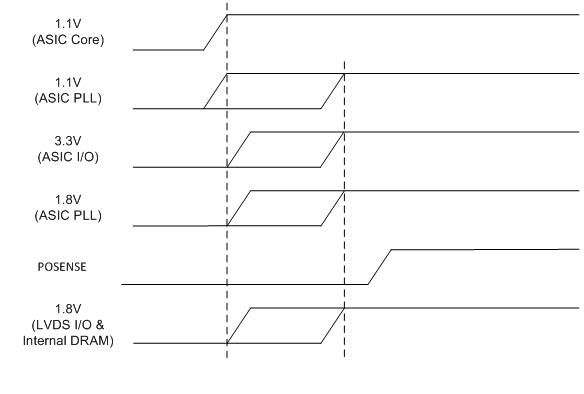
- 1.1V core power is applied whenever any I/O power is applied to ensures the state of the associated I/O that are powered are controlled to a known state. Thus, it is recommended to apply core power first. Other supplies are applied only after the 1.1V core has ramped up.
- All DLPC4420 device power must be applied before POSENSE is asserted to ensure proper power-up initialization.
Typically the DLPC4420 controller power-up sequencing is handled by external hardware. An external power monitor will hold the controller in system reset during power-up (i.e. POSENSE = 0). During this time all DLP controller I/Os are tri-stated. The primary PLL (PLLM1) is released from reset upon the low to high transition of POSENSE but the controller keeps the rest of the device in reset for an additional 60 ms to allow the PLL to lock and stabilize its outputs. After this 60 ms delay the ARM-9 related internal resets are de-asserted causing the microprocessor to begin its boot-up routine.
 Figure 9-1 System Power-Up Sequence