ZHCSLO4D September 2007 – November 2021 DAC5662A
PRODUCTION DATA
- 1 特性
- 2 应用
- 3 描述
- 4 Revision History
- 5 Pin Configurations and Functions
-
6 Specifications
- 6.1 Absolute Maximum Ratings
- 6.2 ESD Ratings
- 6.3 Recommended Operating Conditions
- 6.4 Thermal Resistance Characteristics
- 6.5 Electrical Characteristics
- 6.6 Electrical Characteristics
- 6.7 Electrical Characteristics, AC
- 6.8 Electrical Characteristics, DC
- 6.9 Switching Characteristics
- 6.10 Typical Characteristics
- 7 Parameter Measurement Information
- 8 Detailed Description
- 9 Application and Implementation
- 10Power Supply Recommendations
- 11Layout
- 12Device and Documentation Support
- 13Mechanical, Packaging, and Orderable Information
5 Pin Configurations and Functions
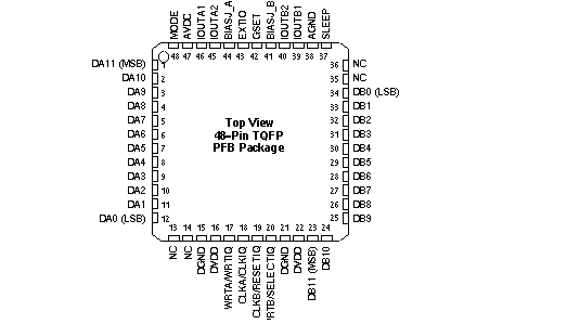
Table 5-1 Pin Functions
| Pin | I/O | DESCRIPTION | |
|---|---|---|---|
| NAME | NO. | ||
| AGND | 38 | I | Analog ground |
| AVDD | 47 | I | Analog supply voltage |
| BIASJ_A | 44 | O | Full-scale output current bias for DACA |
| BIASJ_B | 41 | O | Full-scale output current bias for DACB |
| CLKA/CLKIQ | 18 | I | Clock input for DACA, CLKIQ in interleaved mode. |
| CLKB/RESETIQ | 19 | I | Clock input for DACB, RESETIQ in interleaved mode. |
| DA[11:0] | 1-12 | I | Data port A. DA11 is MSB and DA0 is LSB. Internal pulldown. |
| DB[11:0] | 23-34 | I | Data port B. DB11 is MSB and DB0 is LSB. Internal pulldown. |
| DGND | 15, 21 | I | Digital ground |
| DVDD | 16, 22 | I | Digital supply voltage |
| EXTIO | 43 | I/O | Internal reference output (bypass with 0.1 μF to AGND) or external reference input. |
| GSET | 42 | I | Gain-setting mode: H - 1 resistor, L - 2 resistors. Internal pullup. |
| IOUTA1 | 46 | O | DACA current output. Full-scale with all bits of DA high. |
| IOUTA2 | 45 | O | DACA complementary current output. Full-scale with all bits of DA low. |
| IOUTB1 | 39 | O | DACB current output. Full-scale with all bits of DB high. |
| IOUTB2 | 40 | O | DACB complementary current output. Full-scale with all bits of DB low. |
| MODE | 48 | I | Mode Select: H – Dual Bus, L – Interleaved. Internal pullup. |
| NC | 13, 14, 35, 36 | - | No connection |
| SLEEP | 37 | I | Sleep function control input: H – DAC in power-down mode, L – DAC in operating mode. Internal pulldown. |
| WRTA/WRTIQ | 17 | I | Input write signal for PORT A (WRTIQ in interleaving mode). |
| WRTB/SELECTIQ | 20 | I | Input write signal for PORT B (SELECTIQ in interleaving mode). |