ZHCSLO4D September 2007 – November 2021 DAC5662A
PRODUCTION DATA
- 1 特性
- 2 应用
- 3 描述
- 4 Revision History
- 5 Pin Configurations and Functions
-
6 Specifications
- 6.1 Absolute Maximum Ratings
- 6.2 ESD Ratings
- 6.3 Recommended Operating Conditions
- 6.4 Thermal Resistance Characteristics
- 6.5 Electrical Characteristics
- 6.6 Electrical Characteristics
- 6.7 Electrical Characteristics, AC
- 6.8 Electrical Characteristics, DC
- 6.9 Switching Characteristics
- 6.10 Typical Characteristics
- 7 Parameter Measurement Information
- 8 Detailed Description
- 9 Application and Implementation
- 10Power Supply Recommendations
- 11Layout
- 12Device and Documentation Support
- 13Mechanical, Packaging, and Orderable Information
9.2 Typical Application
A typical application for the DAC5662A is as
dual or single carrier transmitter. The DAC is provided with some input digital baseband
signal and it outputs an analog carrier. A typical configuration is described below.
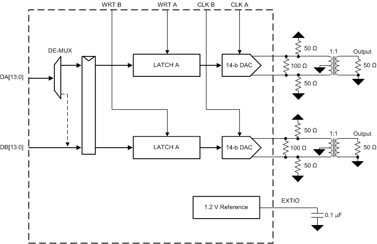
 Figure 9-1 Typical Application
Schematic
 Figure 9-1 Typical Application
Schematic
Figure 9-1 Typical Application
Schematic- Clock rate = 122.88 MHz
- Input data = WCDMA with IF frequency at 30.72 MHz
- AVDD = DVDD = 3.3 V