ZHCSLO4D September   2007  – November 2021 DAC5662A

PRODUCTION DATA  

  1. 特性
  2. 应用
  3. 描述
  4. Revision History
  5. Pin Configurations and Functions
  6. Specifications
    1. 6.1  Absolute Maximum Ratings
    2. 6.2  ESD Ratings
    3. 6.3  Recommended Operating Conditions
    4. 6.4  Thermal Resistance Characteristics
    5. 6.5  Electrical Characteristics
    6. 6.6  Electrical Characteristics
    7. 6.7  Electrical Characteristics, AC
    8. 6.8  Electrical Characteristics, DC
    9. 6.9  Switching Characteristics
    10. 6.10 Typical Characteristics
  7. Parameter Measurement Information
    1. 7.1 Digital Inputs and Timing
      1. 7.1.1 Digital Inputs
      2. 7.1.2 Input Interfaces
      3. 7.1.3 双总线数据接口和时序
      4. 7.1.4 Single-Bus Interleaved Data Interface and Timing
  8. Detailed Description
    1. 8.1 Overview
    2. 8.2 Functional Block Diagram
    3. 8.3 Feature Description
      1. 8.3.1 DAC Transfer Function
      2. 8.3.2 Analog Outputs
      3. 8.3.3 Output Configurations
      4. 8.3.4 Differential With Transformer
      5. 8.3.5 Single-Ended Configuration
      6. 8.3.6 Reference Operation
        1. 8.3.6.1 Internal Reference
        2. 8.3.6.2 External Reference
      7. 8.3.7 Gain Setting Option
    4. 8.4 Device Functional Modes
      1. 8.4.1 Sleep Mode
  9. Application and Implementation
    1. 9.1 Application Informmation
    2. 9.2 Typical Application
      1. 9.2.1 Design Requirements
      2. 9.2.2 Detailed Design Procedure
      3. 9.2.3 Application Curves
  10. 10Power Supply Recommendations
  11. 11Layout
    1. 11.1 Layout Guidelines
    2. 11.2 Layout Example
  12. 12Device and Documentation Support
    1. 12.1 Documentation Support
      1. 12.1.1 Related Documentation
    2. 12.2 接收文档更新通知
    3. 12.3 支持资源
    4. 12.4 Trademarks
    5. 12.5 静电放电警告
    6. 12.6 术语表
  13. 13Mechanical, Packaging, and Orderable Information

封装选项

机械数据 (封装 | 引脚)
散热焊盘机械数据 (封装 | 引脚)
订购信息

DAC Transfer Function

Each of the DACs in the DAC5662A has a set of complementary current outputs, IOUT1 and IOUT2. The full-scale output current, I(OUTFS), is the summation of the two complementary output currents:

Equation 1. GUID-F5D760AE-8F30-47FA-AAAD-881400761BE5-low.gif

The individual output currents depend on the DAC code and can be expressed as:

Equation 2. GUID-48D27510-9E26-4874-B8EF-DAAEB8CC845D-low.gif
Equation 3. GUID-9B7CACA7-BA5E-4D46-9E2B-7BFAB2D9891A-low.gif

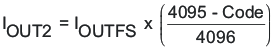
where Code is the decimal representation of the DAC data input word. Additionally, I(OUTFS) is a function of the reference current IREF, which is determined by the reference voltage and the external setting resistor (RSET).

Equation 4. GUID-9C79F06F-2550-4E91-B28E-3EF8670377FD-low.gif

In most cases, the complementary outputs drive resistive loads or a terminated transformer. A signal voltage develops at each output according to:

Equation 5. GUID-92358D3E-3836-4A51-A7CF-65B3AF9B0361-low.gif
Equation 6. GUID-2F7B1D4D-59DF-4FB0-95E7-7580FB775CF8-low.gif

The value of the load resistance is limited by the output compliance specification of the DAC5662A. To maintain specified linearity performance, the voltage for IOUT1 and IOUT2 should not exceed the maximum allowable compliance range.

The total differential output voltage is:

Equation 7. GUID-F5CDD43C-A9D8-476D-A1EF-272399832C2F-low.gif
Equation 8. GUID-605E75DA-FC87-4875-9E84-BC24F18BB26A-low.gif