ZHCS065G March 2011 – January 2024 DAC3482
PRODUCTION DATA
- 1
- 1 特性
- 2 应用
- 3 说明
- 4 Pin Configuration and Functions
-
5 Specifications
- 5.1 Absolute Maximum Ratings
- 5.2 ESD Ratings
- 5.3 Recommended Operating Conditions
- 5.4 Thermal Information
- 5.5 Electrical Characteristics – DC Specifications
- 5.6 Electrical Characteristics – Digital Specifications
- 5.7 Electrical Characteristics – AC Specifications
- 5.8 Electrical Characteristics - Phase-Locked Loop Specifications
- 5.9 Timing Requirements - Digital Specifications
- 5.10 Switching Characteristics – AC Specifications
- 5.11 Typical Characteristics
-
6 Detailed Description
- 6.1 Overview
- 6.2 Functional Block Diagram
- 6.3
Feature Description
- 6.3.1 Serial Interface
- 6.3.2 Data Interface
- 6.3.3 Input FIFO
- 6.3.4 FIFO Modes of Operation
- 6.3.5 Clocking Modes
- 6.3.6 FIR Filters
- 6.3.7 Complex Signal Mixer
- 6.3.8 Quadrature Modulation Correction (QMC)
- 6.3.9 Temperature Sensor
- 6.3.10 Data Pattern Checker
- 6.3.11 Parity Check Test
- 6.3.12 DAC3482 Alarm Monitoring
- 6.3.13 LVPECL Inputs
- 6.3.14 LVDS Inputs
- 6.3.15 Unused LVDS Port Termination
- 6.3.16 CMOS Digital Inputs
- 6.3.17 Reference Operation
- 6.3.18 DAC Transfer Function
- 6.3.19 Analog Current Outputs
- 6.4 Device Functional Modes
- 6.5 Programming
- 6.6
Register Map
- 6.6.1
Register Descriptions
- 6.6.1.1 Register Name: config0 – Address: 0x00, Default: 0x049C
- 6.6.1.2 Register Name: config1 – Address: 0x01, Default: 0x050E
- 6.6.1.3 Register Name: config2 – Address: 0x02, Default: 0x7000
- 6.6.1.4 Register Name: config3 – Address: 0x03, Default: 0xF000
- 6.6.1.5 Register Name: config4 – Address: 0x04, Default: No RESET Value (WRITE TO CLEAR)
- 6.6.1.6 Register Name: config5 – Address: 0x05, Default: Setup and Power-Up Conditions Dependent (WRITE TO CLEAR)
- 6.6.1.7 Register Name: config6 – Address: 0x06, Default: No RESET Value (READ ONLY)
- 6.6.1.8 Register Name: config7 – Address: 0x07, Default: 0xFFFF
- 6.6.1.9 Register Name: config8 – Address: 0x08, Default: 0x0000 (CAUSES AUTO-SYNC)
- 6.6.1.10 Register Name: config9 – Address: 0x09, Default: 0x8000
- 6.6.1.11 Register Name: config10 – Address: 0x0A, Default: 0x0000
- 6.6.1.12 Register Name: config11 – Address: 0x0B, Default: 0x0000
- 6.6.1.13 Register Name: config12 – Address: 0x0C, Default: 0x0400
- 6.6.1.14 Register Name: config13 – Address: 0x0D, Default: 0x0400
- 6.6.1.15 Register Name: config14 – Address: 0x0E, Default: 0x0400
- 6.6.1.16 Register Name: config15 – Address: 0x0F, Default: 0x0400
- 6.6.1.17 Register Name: config16 – Address: 0x10, Default: 0x0000 (CAUSES AUTO-SYNC)
- 6.6.1.18 Register Name: config17 – Address: 0x11, Default: 0x0000
- 6.6.1.19 Register Name: config18 – Address: 0x12, Default: 0x0000 (CAUSES AUTO-SYNC)
- 6.6.1.20 Register Name: config19 – Address: 0x13, Default: 0x0000
- 6.6.1.21 Register Name: config20 – Address: 0x14, Default: 0x0000
- 6.6.1.22 Register Name: config21 – Address: 0x15, Default: 0x0000
- 6.6.1.23 Register name: config22 – Address: 0x16, Default: 0x0000
- 6.6.1.24 Register Name: config23 – Address: 0x17, Default: 0x0000
- 6.6.1.25 Register Name: config24 – Address: 0x18, Default: NA
- 6.6.1.26 Register Name: config25 – Address: 0x19, Default: 0x0440
- 6.6.1.27 Register Name: config26 – Address: 0x1A, Default: 0x0020
- 6.6.1.28 Register Name: config27 – Address: 0x1B, Default: 0x0000
- 6.6.1.29 Register Name: config28 – Address: 0x1C, Default: 0x0000
- 6.6.1.30 Register Name: config29 – Address: 0x1D, Default: 0x0000
- 6.6.1.31 Register Name: config30 – Address: 0x1E, Default: 0x1111
- 6.6.1.32 Register Name: config31 – Address: 0x1F, Default: 0x1140
- 6.6.1.33 Register Name: config32 – Address: 0x20, Default: 0x2400
- 6.6.1.34 Register Name: config33 – Address: 0x21, Default: 0x0000
- 6.6.1.35 Register Name: config34 – Address: 0x22, Default: 0x1B1B
- 6.6.1.36 Register Name: config35 – Address: 0x23, Default: 0xFFFF
- 6.6.1.37 Register Name: config36 – Address: 0x24, Default: 0x0000
- 6.6.1.38 Register Name: config37 – Address: 0x25, Default: 0x7A7A
- 6.6.1.39 Register Name: config38 – Address: 0x26, Default: 0xB6B6
- 6.6.1.40 Register Name: config39 – Address: 0x27, Default: 0xEAEA
- 6.6.1.41 Register Name: config40 – Address: 0x28, Default: 0x4545
- 6.6.1.42 Register Name: config41 – Address: 0x29, Default: 0x1A1A
- 6.6.1.43 Register Name: config42 – Address: 0x2A, Default: 0x1616
- 6.6.1.44 Register Name: config43 – Address: 0x2B, Default: 0xAAAA
- 6.6.1.45 Register Name: config44 – Address: 0x2C, Default: 0xC6C6
- 6.6.1.46 Register Name: config45 – Address: 0x2D, Default: 0x0004
- 6.6.1.47 Register Name: config46 – Address: 0x2E, Default: 0x0000
- 6.6.1.48 Register Name: config47 – Address: 0x2F, Default: 0x0000
- 6.6.1.49 Register Name: config48 – Address: 0x30, Default: 0x0000
- 6.6.1.50 Register Name: version– Address: 0x7F, Default: 0x540C (READ ONLY)
- 6.6.1
Register Descriptions
- 7 Application and Implementation
- 8 Device and Documentation Support
- 9 Revision History
- 10Mechanical, Packaging, and Orderable Information
封装选项
机械数据 (封装 | 引脚)
散热焊盘机械数据 (封装 | 引脚)
- RKD|88
订购信息
6.3.6 FIR Filters
Figure 6-12 through Figure 6-15 show the magnitude spectrum response for the FIR0, FIR1, FIR2, and FIR3 interpolating filters where fIN is the input data rate to the FIR filter. Figure 6-16 to Figure 6-19 show the composite filter response for 2x, 4x, 8x, and 16x interpolation. The transition band for all interpolation settings is from 0.4 to 0.6 x fDATA (the input data rate to the device) with < 0.001dB of pass-band ripple and > 90dB stop-band attenuation.
The DAC3482 also has a 9-tap inverse sinc filter (FIR4) that runs at the DAC update rate (fDAC) that can be used to flatten the frequency response of the sample-and-hold output. The DAC sample-and-hold output sets the output current and holds it constant for one DAC clock cycle until the next sample, resulting in the well-known sin(x)/x or sinc(x) frequency response (Figure 6-20, red line). The inverse sinc filter response (Figure 6-20, blue line) has the opposite frequency response from 0 to 0.4 x fDAC, resulting in the combined response (Figure 6-20, green line). Between 0 to 0.4 x fDAC, the inverse sinc filter compensates the sample-and-hold roll-off with less than 0.03dB error.
The inverse sinc filter has a gain > 1 at all frequencies. Therefore, the signal input to FIR4 must be reduced from full scale to prevent saturation in the filter. The amount of back-off required depends on the signal frequency, and is set such that at the signal frequencies the combination of the input signal and filter response is less than 1 (0dB). For example, if the signal input to FIR4 is at 0.25 x fDAC, the response of FIR4 is 0.9dB, and the signal must be backed off from full scale by 0.9dB to avoid saturation. The gain function in the QMC blocks can be used to reduce the amplitude of the input signal. The advantage of FIR4 having a positive gain at all frequencies is that the user is then able to optimize the back-off of the signal based on its frequency.
The filter taps for all digital filters are listed in Table 6-6. Note that the loss of signal amplitude may result in lower SNR due to decrease in signal amplitude.
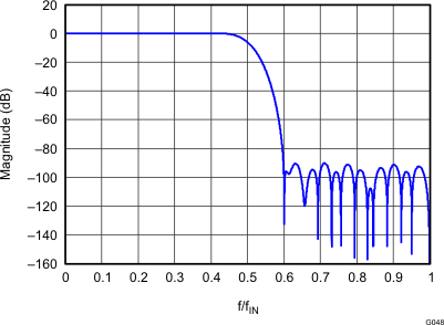 Figure 6-12 Magnitude Spectrum for FIR0
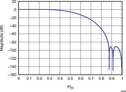 Figure 6-14 Magnitude Spectrum for FIR2
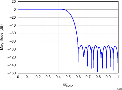 Figure 6-16 2x Interpolation Composite Response
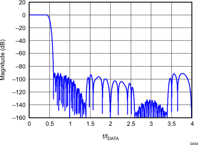 Figure 6-18 8x Interpolation Composite Response
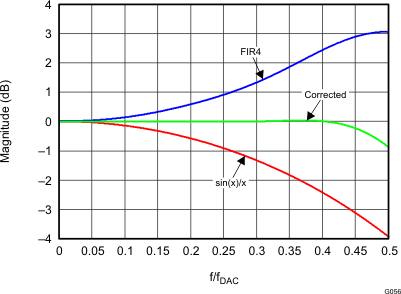 Figure 6-20 Magnitude Spectrum for Inverse Sinc Filter
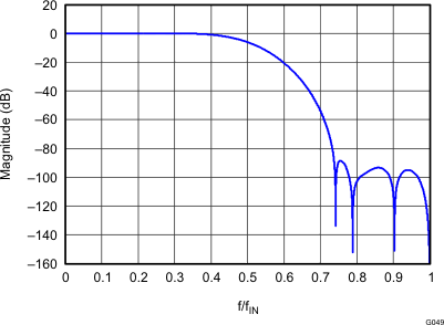 Figure 6-13 Magnitude Spectrum for FIR1
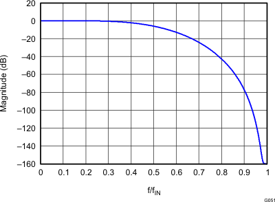 Figure 6-15 Magnitude Spectrum for FIR3
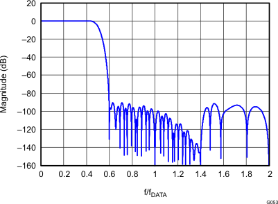 Figure 6-17 4x Interpolation Composite Response
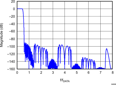 Figure 6-19 16x Interpolation Composite Response
| INTERPOLATING HALF-BAND FILTERS | NON-INTERPOLATING INVERSE-SINC Filter | ||||||||
|---|---|---|---|---|---|---|---|---|---|
| FIR0 | FIR1 | FIR2 | FIR3 | FIR4 | |||||
| 59 TAPS | 23 TAPS | 11 TAPS | 11 TAPS | 9 TAPS | |||||
| 6 | 6 | -12 | -12 | 29 | 29 | 3 | 3 | 1 | 1 |
| 0 | 0 | 0 | 0 | 0 | 0 | 0 | 0 | -4 | -4 |
| -19 | -19 | 84 | 84 | -214 | -214 | -25 | -25 | 13 | 13 |
| 0 | 0 | 0 | 0 | 0 | 0 | 0 | 0 | -50 | -50 |
| 47 | 47 | -336 | -336 | 1209 | 1209 | 150 | 150 | 592(1) | |
| 0 | 0 | 0 | 0 | 2048(1) | 256(1) | ||||
| -100 | -100 | 1006 | 1006 | ||||||
| 0 | 0 | 0 | 0 | ||||||
| 192 | 192 | -2691 | -2691 | ||||||
| 0 | 0 | 0 | 0 | ||||||
| -342 | -342 | 10141 | 10141 | ||||||
| 0 | 0 | 16384(1) | |||||||
| 572 | 572 | ||||||||
| 0 | 0 | ||||||||
| -914 | -914 | ||||||||
| 0 | 0 | ||||||||
| 1409 | 1409 | ||||||||
| 0 | 0 | ||||||||
| -2119 | -2119 | ||||||||
| 0 | 0 | ||||||||
| 3152 | 3152 | ||||||||
| 0 | 0 | ||||||||
| -4729 | -4729 | ||||||||
| 0 | 0 | ||||||||
| 7420 | 7420 | ||||||||
| 0 | 0 | ||||||||
| -13334 | -13334 | ||||||||
| 0 | 0 | ||||||||
| 41527 | 41527 | ||||||||
| 65536(1) | |||||||||