ZHCSDZ0B July 2015 – January 2022 TUSB4020BI-Q1
PRODUCTION DATA
- 1 特性
- 2 应用
- 3 说明
- 4 Revision History
- 5 说明(续)
- 6 Pin Configuration and Functions
- 7 Specifications
-
8 Detailed Description
- 8.1 Overview
- 8.2 Functional Block Diagram
- 8.3 Feature Description
- 8.4 Device Functional Modes
- 8.5 Programming
- 8.6
Register Maps
- 8.6.1
Configuration Registers
- 8.6.1.1 ROM Signature Register (offset = 0h) [reset = 0h]
- 8.6.1.2 Vendor ID LSB Register (offset = 1h) [reset = 51h]
- 8.6.1.3 Vendor ID MSB Register (offset = 2h) [reset = 4h]
- 8.6.1.4 Product ID LSB Register (offset = 3h) [reset = 25h]
- 8.6.1.5 Product ID MSB Register (offset = 4h) [reset = 80h]
- 8.6.1.6 Device Configuration Register (offset = 5h) [reset = 1Xh]
- 8.6.1.7 Battery Charging Support Register (offset = 6h) [reset = 0Xh]
- 8.6.1.8 Device Removable Configuration Register (offset = 7h) [reset = 0Xh]
- 8.6.1.9 Port Used Configuration Register (offset = 8h) [reset = 0h]
- 8.6.1.10 PHY Custom Configuration Register (offset = 9h) [reset = 0h]
- 8.6.1.11 Device Configuration Register 2 (offset = Ah)
- 8.6.1.12 UUID Registers (offset = 10h to 1Fh)
- 8.6.1.13 Language ID LSB Register (offset = 20h)
- 8.6.1.14 Language ID MSB Register (offset = 21h)
- 8.6.1.15 Serial Number String Length Register (offset = 22h)
- 8.6.1.16 Manufacturer String Length Register (offset = 23h)
- 8.6.1.17 Product String Length Register (offset = 24h)
- 8.6.1.18 Serial Number Registers (offset = 30h to 4Fh)
- 8.6.1.19 Manufacturer String Registers (offset = 50h to 8Fh)
- 8.6.1.20 Product String Registers (offset = 90h to CFh)
- 8.6.1.21 Additional Feature Configuration Register (offset = F0h)
- 8.6.1.22 Charging Port Control Register (offset = F2h)
- 8.6.1.23 Device Status and Command Register (offset = F8h)
- 8.6.1
Configuration Registers
- 9 Application and Implementation
- 10Power Supply Recommendations
- 11Layout
- 12Device and Documentation Support
- 13Mechanical, Packaging, and Orderable Information
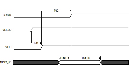
7.7 Power-Up Timing Requirements
| MIN | NOM | MAX | UNIT | ||
|---|---|---|---|---|---|
| td1 | VDD33 stable before VDD stable(1) | see (2) | ms | ||
| td2 | VDD and VDD33 stable before deassertion of GRSTz | 3 | ms | ||
| tsu_io | Setup for MISC inputs(3) sampled at the deassertion of GRSTz | 0.1 | µs | ||
| thd_io | Hold for MISC inputs(3) sampled at the deassertion of GRSTz. | 0.1 | µs | ||
| tVDD33_RAMP | VDD33 supply ramp requirements | 0.2 | 100 | ms | |
| tVDD_RAMP | VDD supply ramp requirements | 0.2 | 100 | ms | |
(1) An active reset is required if the VDD33 supply is stable before the VDD11 supply. This active Reset shall meet the 3ms power-up delay counting from both power supplies being stable to the de-assertion of GRSTz.
(2) There is no power-on relationship between VDD33 and VDD unless GRSTz is only connected to a capacitor to GND. Then VDD must be stable minimum of 10 μs before the VDD33.
(3) MISC pins sampled at deassertion of GRSTz: FULLPWRMGMTz, GANGED, PWRCTL_POL, SMBUSz, BATEN[4:1], and AUTOENz.
 Figure 7-1 Power-Up Timing Requirements