ZHCSE41C August 2015 – May 2017 LP8861-Q1
PRODUCTION DATA.
- 1 特性
- 2 应用
- 3 说明
- 4 修订历史记录
- 5 器件比较表
- 6 Pin Configuration and Functions
-
7 Specifications
- 7.1 Absolute Maximum Ratings
- 7.2 ESD Ratings
- 7.3 Recommended Operating Conditions
- 7.4 Thermal Information
- 7.5 Electrical Characteristics
- 7.6 Internal LDO Electrical Characteristics
- 7.7 Protection Electrical Characteristics
- 7.8 Power Line FET Control Electrical Characteristics
- 7.9 Current Sinks Electrical Characteristics
- 7.10 PWM Brightness Control Electrical Characteristics
- 7.11 Boost/SEPIC Converter Characteristics
- 7.12 Logic Interface Characteristics
- 7.13 Typical Characteristics
-
8 Detailed Description
- 8.1 Overview
- 8.2 Functional Block Diagram
- 8.3 Feature Description
- 8.4 Device Functional Modes
-
9 Application and Implementation
- 9.1 Application Information
- 9.2 Typical Applications
- 10Power Supply Recommendations
- 11Layout
- 12器件和文档支持
- 13机械、封装和可订购信息
8.3.5 LED Current Dimming With External Temperature Sensor
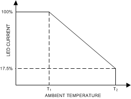
The LP8861-Q1 has an optional feature to decrease automatically LED current when LED overheating is detected with an external NTC sensor. An example of the behavior is shown in Figure 11. When the NTC temperature reaches T1, the LP8861-Q1 starts to decrease the LED current. When the LED current has reduced to 17.5% of the nominal value, current turns off until temperature returns to the operation range. When TSET pin is grounded this feature is disabled. Temperature T1 and de-rate slope are defined by external resistors as explained below.
 Figure 11. Temperature-Based LED Current Dimming Functionality
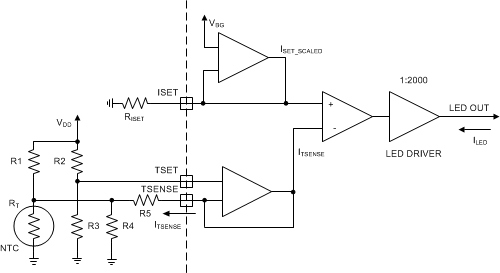
  Figure 12. Temperature-Based LED Current Dimming Implementation
 When the TSET pin is grounded LED current is set by RISET resistor:

When external NTC is connected, the TSENSE pin current decreases LED output current. The following steps describe how to calculate LED output current.
Parallel resistance of the NTC sensor RT and resistor R4 is calculated by formula:

TSET voltage can be calculated with Equation 6:

TSENSE pin current is calculated by Equation 7:

ISET pin current defined by RISET is:

For Equation 9, ITSENSE current must be limited between 0 and ISET_SCALED. If ITSENSE > ISET_SCALED then set ITSENSE = ISET_SCALED. If ITSENSE < 0 then set ITSENSE = 0.
LED driver output current is:
When current is lower than 17.5% of the nominal value, the current is set to 0 (so called cut-off point).
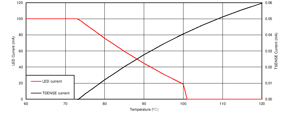
An Excel® calculator is available for calculating the component values for a specific NTC and target thermal profile (contact your local TI representative). Figure 13 shows an example thermal profile implementation.

| NTC – 10 kΩ at 25ºC | RISET = 24 kΩ | R2 = 10 kΩ | R4 = 100 kΩ |
| VDD = 4.3 V | R1 = 10 kΩ | R3 = 2 kΩ | R5 = 7.5 kΩ |