ZHCSIA3C Februray   2017  – May 2018 LMK04832

PRODUCTION DATA.  

  1. 特性
  2. 应用
  3. 说明
    1.     简化原理图
  4. 修订历史记录
  5. Pin Configuration and Functions
    1.     Pin Functions
  6. Specifications
    1. 6.1 Absolute Maximum Ratings
    2. 6.2 ESD Ratings
    3. 6.3 Recommended Operating Conditions
    4. 6.4 Thermal Information
    5. 6.5 Electrical Characteristics
    6. 6.6 Timing Requirements
    7. 6.7 Timing Diagram
    8. 6.8 Typical Characteristics – Clock Output AC Characteristics
  7. Parameter Measurement Information
    1. 7.1 Charge Pump Current Specification Definitions
      1. 7.1.1 Charge Pump Output Current Magnitude Variation vs Charge Pump Output Voltage
      2. 7.1.2 Charge Pump Sink Current vs Charge Pump Output Source Current Mismatch
      3. 7.1.3 Charge Pump Output Current Magnitude Variation vs Ambient Temperature
    2. 7.2 Differential Voltage Measurement Terminology
  8. Detailed Description
    1. 8.1 Overview
      1. 8.1.1  Differences to LMK0482x
      2. 8.1.2  Jitter Cleaning
      3. 8.1.3  JEDEC JESD204B Support
      4. 8.1.4  Clock Inputs
        1. 8.1.4.1 Three Redundant PLL1 Reference Inputs
        2. 8.1.4.2 PLL2 Reference Inputs
        3. 8.1.4.3 Clock Distribution Reference Input
      5. 8.1.5  VCXO Buffered Output
      6. 8.1.6  Frequency Holdover
      7. 8.1.7  Internal VCOs
      8. 8.1.8  External VCO Mode
      9. 8.1.9  Clock Distribution
        1. 8.1.9.1 Clock Divider
        2. 8.1.9.2 High Performance Divider Bypass Mode
        3. 8.1.9.3 SYSREF Clock Divider
        4. 8.1.9.4 Device Clock Delay
        5. 8.1.9.5 Dynamic Digital Delay
        6. 8.1.9.6 SYSREF Delay: Global and Local
        7. 8.1.9.7 Programmable Output Formats
        8. 8.1.9.8 Clock Output Synchronization
      10. 8.1.10 0-Delay
      11. 8.1.11 Status Pins
    2. 8.2 Functional Block Diagram
    3. 8.3 Feature Description
      1. 8.3.1 Synchronizing PLL R Dividers
        1. 8.3.1.1 PLL1 R Divider Synchronization
        2. 8.3.1.2 PLL2 R Divider Synchronization
      2. 8.3.2 SYNC/SYSREF
      3. 8.3.3 JEDEC JESD204B
        1. 8.3.3.1 How to Enable SYSREF
          1. 8.3.3.1.1 Setup of SYSREF Example
          2. 8.3.3.1.2 SYSREF_CLR
        2. 8.3.3.2 SYSREF Modes
          1. 8.3.3.2.1 SYSREF Pulser
          2. 8.3.3.2.2 Continuous SYSREF
          3. 8.3.3.2.3 SYSREF Request
      4. 8.3.4 Digital Delay
        1. 8.3.4.1 Fixed Digital Delay
          1. 8.3.4.1.1 Fixed Digital Delay Example
        2. 8.3.4.2 Dynamic Digital Delay
        3. 8.3.4.3 Single and Multiple Dynamic Digital Delay Example
      5. 8.3.5 SYSREF to Device Clock Alignment
      6. 8.3.6 Input Clock Switching
        1. 8.3.6.1 Input Clock Switching - Manual Mode
        2. 8.3.6.2 Input Clock Switching - Pin Select Mode
        3. 8.3.6.3 Input Clock Switching - Automatic Mode
      7. 8.3.7 Digital Lock Detect
        1. 8.3.7.1 Calculating Digital Lock Detect Frequency Accuracy
      8. 8.3.8 Holdover
        1. 8.3.8.1 Enable Holdover
          1. 8.3.8.1.1 Fixed (Manual) CPout1 Holdover Mode
          2. 8.3.8.1.2 Tracked CPout1 Holdover Mode
        2. 8.3.8.2 During Holdover
        3. 8.3.8.3 Exiting Holdover
        4. 8.3.8.4 Holdover Frequency Accuracy and DAC Performance
      9. 8.3.9 PLL2 Loop Filter
    4. 8.4 Device Functional Modes
      1. 8.4.1 DUAL PLL
        1. 8.4.1.1 Dual Loop
        2. 8.4.1.2 Dual Loop With Cascaded 0-Delay
        3. 8.4.1.3 Dual Loop With Nested 0-Delay
      2. 8.4.2 Single PLL
        1. 8.4.2.1 PLL2 Single Loop
        2. 8.4.2.2 PLL2 With External VCO
      3. 8.4.3 Distribution Mode
    5. 8.5 Programming
      1. 8.5.1 Recommended Programming Sequence
    6. 8.6 Register Maps
      1. 8.6.1 Register Map for Device Programming
      2. 8.6.2 Device Register Descriptions
        1. 8.6.2.1 System Functions
          1. 8.6.2.1.1 RESET, SPI_3WIRE_DIS
          2. 8.6.2.1.2 POWERDOWN
          3. 8.6.2.1.3 ID_DEVICE_TYPE
          4. 8.6.2.1.4 ID_PROD
          5. 8.6.2.1.5 ID_MASKREV
          6. 8.6.2.1.6 ID_VNDR
        2. 8.6.2.2 (0x100 - 0x138) Device Clock and SYSREF Clock Output Controls
          1. 8.6.2.2.1 DCLKX_Y_DIV
          2. 8.6.2.2.2 DCLKX_Y_DDLY
          3. 8.6.2.2.3 CLKoutX_Y_PD, CLKoutX_Y_ODL, CLKoutX_Y_IDL, DCLKX_Y_DDLY_PD, DCLKX_Y_DDLY[9:8], DCLKX_Y_DIV[9:8]
          4. 8.6.2.2.4 CLKoutX_SRC_MUX, CLKoutX_Y_PD, DCLKX_Y_BYP, DCLKX_Y_DCC, DCLKX_Y_POL, DCLKX_Y_HS
          5. 8.6.2.2.5 CLKoutY_SRC_MUX, SCLKX_Y_PD, SCLKX_Y_DIS_MODE, SCLKX_Y_POL, SCLKX_Y_HS
          6. 8.6.2.2.6 SCLKX_Y_ADLY_EN, SCLKX_Y_ADLY
          7. 8.6.2.2.7 SCLKX_Y_DDLY
          8. 8.6.2.2.8 CLKoutY_FMT, CLKoutX_FMT
        3. 8.6.2.3 SYSREF, SYNC, and Device Config
          1. 8.6.2.3.1  VCO_MUX, OSCout_MUX, OSCout_FMT
          2. 8.6.2.3.2  SYSREF_REQ_EN, SYNC_BYPASS, SYSREF_MUX
          3. 8.6.2.3.3  SYSREF_DIV
          4. 8.6.2.3.4  SYSREF_DDLY
          5. 8.6.2.3.5  SYSREF_PULSE_CNT
          6. 8.6.2.3.6  PLL2_RCLK_MUX, PLL2_NCLK_MUX, PLL1_NCLK_MUX, FB_MUX, FB_MUX_EN
          7. 8.6.2.3.7  PLL1_PD, VCO_LDO_PD, VCO_PD, OSCin_PD, SYSREF_GBL_PD, SYSREF_PD, SYSREF_DDLY_PD, SYSREF_PLSR_PD
          8. 8.6.2.3.8  DDLYdSYSREF_EN, DDLYdX_EN
          9. 8.6.2.3.9  DDLYd_STEP_CNT
          10. 8.6.2.3.10 SYSREF_CLR, SYNC_1SHOT_EN, SYNC_POL, SYNC_EN, SYNC_PLL2_DLD, SYNC_PLL1_DLD, SYNC_MODE
          11. 8.6.2.3.11 SYNC_DISSYSREF, SYNC_DISX
          12. 8.6.2.3.12 PLL1R_SYNC_EN, PLL1R_SYNC_SRC, PLL2R_SYNC_EN
        4. 8.6.2.4 (0x146 - 0x149) CLKin Control
          1. 8.6.2.4.1 CLKin_SEL_PIN_EN, CLKin_SEL_PIN_POL, CLKin2_EN, CLKin1_EN, CLKin0_EN, CLKin2_TYPE, CLKin1_TYPE, CLKin0_TYPE
          2. 8.6.2.4.2 CLKin_SEL_AUTO_REVERT_EN, CLKin_SEL_AUTO_EN, CLKin_SEL_MANUAL, CLKin1_DEMUX, CLKin0_DEMUX
          3. 8.6.2.4.3 CLKin_SEL0_MUX, CLKin_SEL0_TYPE
          4. 8.6.2.4.4 SDIO_RDBK_TYPE, CLKin_SEL1_MUX, CLKin_SEL1_TYPE
        5. 8.6.2.5 RESET_MUX, RESET_TYPE
        6. 8.6.2.6 (0x14B - 0x152) Holdover
          1. 8.6.2.6.1 LOS_TIMEOUT, LOS_EN, TRACK_EN, HOLDOVER_FORCE, MAN_DAC_EN, MAN_DAC[9:8]
          2. 8.6.2.6.2 MAN_DAC
          3. 8.6.2.6.3 DAC_TRIP_LOW
          4. 8.6.2.6.4 DAC_CLK_MULT, DAC_TRIP_HIGH
          5. 8.6.2.6.5 DAC_CLK_CNTR
          6. 8.6.2.6.6 CLKin_OVERRIDE, HOLDOVER_EXIT_MODE, HOLDOVER_PLL1_DET, LOS_EXTERNAL_INPUT, HOLDOVER_VTUNE_DET, CLKin_SWITCH_CP_TRI, HOLDOVER_EN
          7. 8.6.2.6.7 HOLDOVER_DLD_CNT
        7. 8.6.2.7 (0x153 - 0x15F) PLL1 Configuration
          1. 8.6.2.7.1 CLKin0_R
          2. 8.6.2.7.2 CLKin1_R
          3. 8.6.2.7.3 CLKin2_R
          4. 8.6.2.7.4 PLL1_N
          5. 8.6.2.7.5 PLL1_WND_SIZE, PLL1_CP_TRI, PLL1_CP_POL, PLL1_CP_GAIN
          6. 8.6.2.7.6 PLL1_DLD_CNT
          7. 8.6.2.7.7 HOLDOVER_EXIT_NADJ
          8. 8.6.2.7.8 PLL1_LD_MUX, PLL1_LD_TYPE
        8. 8.6.2.8 (0x160 - 0x16E) PLL2 Configuration
          1. 8.6.2.8.1 PLL2_R
          2. 8.6.2.8.2 PLL2_P, OSCin_FREQ, PLL2_REF_2X_EN
          3. 8.6.2.8.3 PLL2_N_CAL
          4. 8.6.2.8.4 PLL2_N
          5. 8.6.2.8.5 PLL2_WND_SIZE, PLL2_CP_GAIN, PLL2_CP_POL, PLL2_CP_TRI
          6. 8.6.2.8.6 PLL2_DLD_CNT
          7. 8.6.2.8.7 PLL2_LD_MUX, PLL2_LD_TYPE
        9. 8.6.2.9 (0x16F - 0x555) Misc Registers
          1. 8.6.2.9.1 PLL2_PRE_PD, PLL2_PD
          2. 8.6.2.9.2 PLL1R_RST
          3. 8.6.2.9.3 CLR_PLL1_LD_LOST, CLR_PLL2_LD_LOST
          4. 8.6.2.9.4 RB_PLL1_LD_LOST, RB_PLL1_LD, RB_PLL2_LD_LOST, RB_PLL2_LD
          5. 8.6.2.9.5 RB_DAC_VALUE (MSB), RB_CLKinX_SEL, RB_CLKinX_LOS
          6. 8.6.2.9.6 RB_DAC_VALUE
          7. 8.6.2.9.7 RB_HOLDOVER
          8. 8.6.2.9.8 SPI_LOCK
  9. Application and Implementation
    1. 9.1 Application Information
      1. 9.1.1 Digital Lock Detect Frequency Accuracy
        1. 9.1.1.1 Minimum Lock Time Calculation Example
      2. 9.1.2 Driving CLKin AND OSCin Inputs
        1. 9.1.2.1 Driving CLKin and OSCin PINS With a Differential Source
        2. 9.1.2.2 Driving CLKin Pins With a Single-Ended Source
      3. 9.1.3 OSCin Doubler for Best Phase Noise Performance
    2. 9.2 Typical Application
      1. 9.2.1 Design Requirements
      2. 9.2.2 Detailed Design Procedure
        1. 9.2.2.1 Device Selection
          1. 9.2.2.1.1 Clock Architect
        2. 9.2.2.2 Device Configuration and Simulation
        3. 9.2.2.3 Device Programming
      3. 9.2.3 Application Curves
    3. 9.3 Do's and Don'ts
      1. 9.3.1 Pin Connection Recommendations
  10. 10Power Supply Recommendations
    1. 10.1 Current Consumption
  11. 11Layout
    1. 11.1 Layout Guidelines
      1. 11.1.1 Thermal Management
    2. 11.2 Layout Example
  12. 12器件和文档支持
    1. 12.1 器件支持
      1. 12.1.1 开发支持
        1. 12.1.1.1 时钟架构
        2. 12.1.1.2 PLLatinum 仿真
        3. 12.1.1.3 TICS Pro
    2. 12.2 社区资源
    3. 12.3 商标
    4. 12.4 静电放电警告
    5. 12.5 术语表
  13. 13机械、封装和可订购信息

封装选项

机械数据 (封装 | 引脚)
散热焊盘机械数据 (封装 | 引脚)
订购信息

Differential Voltage Measurement Terminology

The differential voltage of a differential signal can be described by two different definitions causing confusion when reading data sheets or communicating with other engineers. This section will address the measurement and description of a differential signal so that the reader will be able to understand and distinguish between the two different definitions when used.

The first definition used to describe a differential signal is the absolute value of the voltage potential between the inverting and noninverting signal. The symbol for this first measurement is typically VID or VOD depending on if an input or output voltage is being described.

The second definition used to describe a differential signal is to measure the potential of the noninverting signal with respect to the inverting signal. The symbol for this second measurement is VSS and is a calculated parameter. Nowhere in the IC does this signal exist with respect to ground, it only exists in reference to its differential pair. VSS can be measured directly by oscilloscopes with floating references, otherwise this value can be calculated as twice the value of VOD as described in the first description.

Figure 4 illustrates the two different definitions side-by-side for inputs and Figure 5 illustrates the two different definitions side-by-side for outputs. The VID and VOD definitions show VA and VB DC levels that the noninverting and inverting signals toggle between with respect to ground. VSS input and output definitions show that if the inverting signal is considered the voltage potential reference, the noninverting signal voltage potential is now increasing and decreasing above and below the noninverting reference. Thus the peak-to-peak voltage of the differential signal can be measured.

VID and VOD are often defined as volts (V) and VSS is often defined as volts peak-to-peak (VPP).
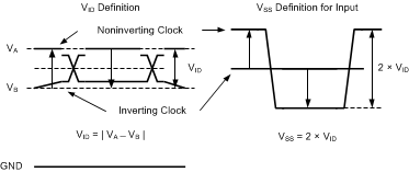
LMK04832 30189075.gifFigure 4. Two Different Definitions for
Differential Input Signals
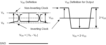
LMK04832 30189074.gifFigure 5. Two Different Definitions for
Differential Output Signals

Refer to application note AN-912 Common Data Transmission Parameters and their Definitions (SNLA036) for more information.