TIDUEM7A April 2019 – February 2021
- Description
- Resources
- Features
- Applications
- 5
- 1System Description
-
2System Overview
- 2.1 Block Diagram
- 2.2 Highlighted Products
- 2.3 Design Considerations
- 2.4
Hardware, Software, Testing Requirements, and Test Results
- 2.4.1 Required Hardware and Software
- 2.4.2
Testing and Results
- 2.4.2.1 Test Setup
- 2.4.2.2 Test Results
- 3Design Files
- 4Related Documentation
- 5About the Author
- 6Revision History
2.4.1.2.1 Connections to the Test Setup
AC voltages and currents can be applied to the board for testing purposes at these points:
- Terminal block "J22" is a two-position terminal block that corresponds to the line and neutral voltage connection. If referencing the shunt and system ground with respect to the neutral, connect the terminal block position on the left, which is labeled "NEG", to the neutral and connect the terminal block position on the right, which is labeled "POS", to the line. If referencing the shunt and system ground with respect to the line, connect the terminal block position on the left, which is labeled "NEG", to the line and connect the terminal block position on the right, which is labeled "POS", to the neutral. If the system is referenced with respect to the line, note that all voltage samples obtained from the ADS131M04 should be multiplied by –1 in the software to ensure that the phase shift between voltage and current is properly reflected for the power-related metrology readings.
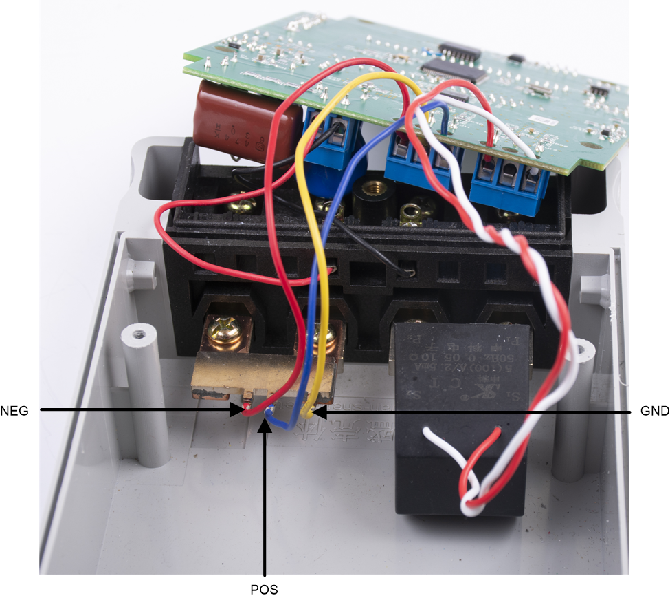
- Terminal block "J25" is connected to the output terminals of the shunt. This terminal block is a three-position terminal block with positions labeled "POS", "GND", and "NEG". For the gain of 32 used in this design, the differential voltage across the "POS" and "NEG" terminals of this terminal block should be less than ±37.5 mV. Do not connect a CT here since a burden resistor is not present for the circuitry of this channel like it is present for the J26 current circuitry. Figure 2-25 shows a mapping between shunt terminals and the positions on J25. The differential voltage output from the shunt, which is fed to the POS and NEG positions of J25, should not exceed ±37.5 mV.
- Terminal block "J26" corresponds to the current inputs after the CT. This terminal block is a three-position terminal block but only the leftmost and rightmost positions are used. The center position, which is connected to GND, is not connected to the CT. Connect the positive terminal of the CT to the terminal block position (labeled "POS") on the most right. Connect the negative terminal of the CT to the terminal block position (labeled "NEG") on the most left. Select the applied current to the input of the CT so that it does not exceed 100 A. In addition, before performing any test, verify that this terminal block is securely connected to both output leads of the CT.
 Figure 2-25 Mapping Between Shunt Terminals and J25 Terminal Block Positions
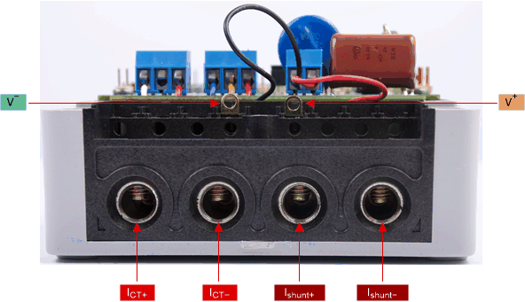
Figure 2-26 shows the various test setup connections required for the reference design to function properly. If the shunt and system is referenced with respect to the neutral, V+ corresponds to the line connection and V- corresponds to the neutral connection. If the shunt and system is referenced with respect to the line, V+ corresponds to the neutral connection and V- corresponds to the line connection.
Ishunt+ and Ishunt- correspond to the current inputs to the shunt of the design while ICT+, and ICT- correspond to the current inputs to the current transformer of the design.
 Figure 2-26 View of Reference Design With Test Setup Connections