TIDUEM7A April 2019 – February 2021
- Description
- Resources
- Features
- Applications
- 5
- 1System Description
-
2System Overview
- 2.1 Block Diagram
- 2.2 Highlighted Products
- 2.3 Design Considerations
- 2.4
Hardware, Software, Testing Requirements, and Test Results
- 2.4.1 Required Hardware and Software
- 2.4.2
Testing and Results
- 2.4.2.1 Test Setup
- 2.4.2.2 Test Results
- 3Design Files
- 4Related Documentation
- 5About the Author
- 6Revision History
2.1 Block Diagram
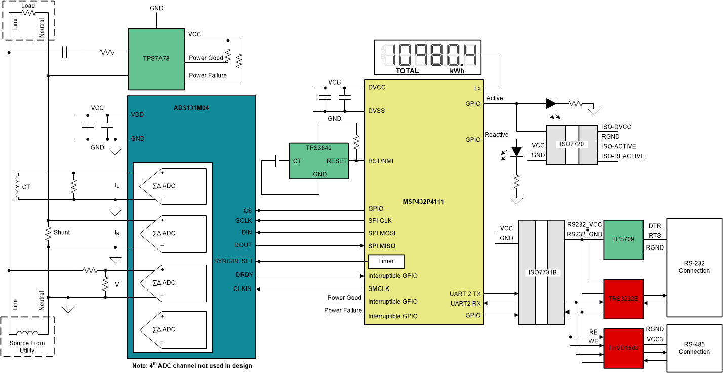
Figure 2-1 depicts a block diagram that shows the high-level interface used for an ADS131M04-based one-phase energy measurement application.
 Figure 2-1 TIDA-010036 Block
Diagram
Figure 2-1 TIDA-010036 Block
DiagramIn Figure 2-1, a simple voltage divider is used for translating the Mains voltage to a voltage that can be sensed by the ADC. For the current, two current sensors are used, where one current sensor is used for sensing the line current and another current sensor is used to sense the neutral current. The design uses a shunt and a current transformer for the current sensors. In Figure 2-1, the system shows that the CT measures the line current, the shunt measures the neutral current, and the system is referenced with respect to the neutral; however, the design also supports a second configuration where the CT measures the neutral current, the shunt measures the line current, and the system is referenced with respect to the line.
For the shunt current sensor, the resistance of the shunt is selected based on the current range required for energy measurements and also the minimization of the maximum power dissipation of the shunt. For the CT current sensor, the CT has an associated burden resistor that must be connected at all times to protect the measuring device. The selection of the CT and the burden resistor is made based on the manufacturer and current range required for energy measurements.
The choice of voltage divider resistors for the voltage channel is selected to ensure the Mains voltage is divided down to adhere to the normal input ranges of the ADS131M04 device. Since the ADS131M04 ADCs have a large dynamic range and a large dynamic range is not needed to measure voltage, the voltage front-end circuitry is purposely selected so that the maximum voltage seen at the inputs of the voltage channel ADCs are only a fraction of the full-scale voltage. By reducing the voltage fed to the ADS131M04 voltage ADC, voltage-to-current crosstalk, which actually affects metrology accuracy more than voltage ADC accuracy, is reduced at the cost of voltage accuracy.
In this design, the ADS131M04 device interacts with the MSP432™ MCU in the following manner:
- The CLKIN clock used by the ADS131M04 device is provided from the SMCLK clock signal output of the MSP432 MCU.
- The ADS131M04 device divides the clock provided on its CLKIN pin by two and uses this divided clock as its delta-sigma modulation clock.
- When new ADC samples are ready, the ADS131M04 device asserts its DRDY pin, which alerts the MSP432 MCU that new samples are available.
- After being alerted of new samples, the MSP432 MCU uses one of its SPI interfaces and its DMA to get the voltage and current samples from the ADS131M04 device.
In this design, a TPS3840 device is used as an external SVS for the MSP432 MCU. Although the MSP432 MCU has an internal SVS that suffices for this application, the TPS3840 standalone SVS is used because there is additional security in having an SVS that is independent of the MCU.
To power this design, a TPS7A78 device is used to implement a cap-drop supply. This TPS7A78 device allows a higher output current than traditional cap-drop supplies. It also has a power failure pin, which can be used to alert the MCU whenever the system sees an AC supply failure either because of a power outage or if the neutral connection has been removed from the meter. The TPS7A78 has a power good pin, which can be used to alert the MCU that the output voltage of the cap-drop supply has ramped up after power has been restored from a power outage.
Other signals of interest in Figure 2-1 are the active and reactive energy pulses used for accuracy measurement and calibration. The ISO7720 device provides an isolated connection for these pulses for connecting to non-isolated equipment. This is especially needed if the shunt measures the line current since the system is referenced to this high-voltage line connection as well for this configuration.
In addition to isolated pulses, the design supports isolated RS-232 communication through the use of the TPS70933, ISO7731B, and TRS3232E devices. The design can be configured to use RS-485 as well instead of RS-232 through the use of the ISO7731B and THVD1500 devices on the board.