TIDT228 October 2022
3.1 Switching
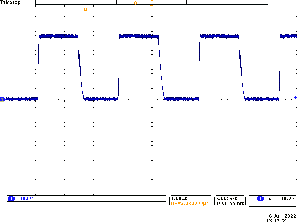
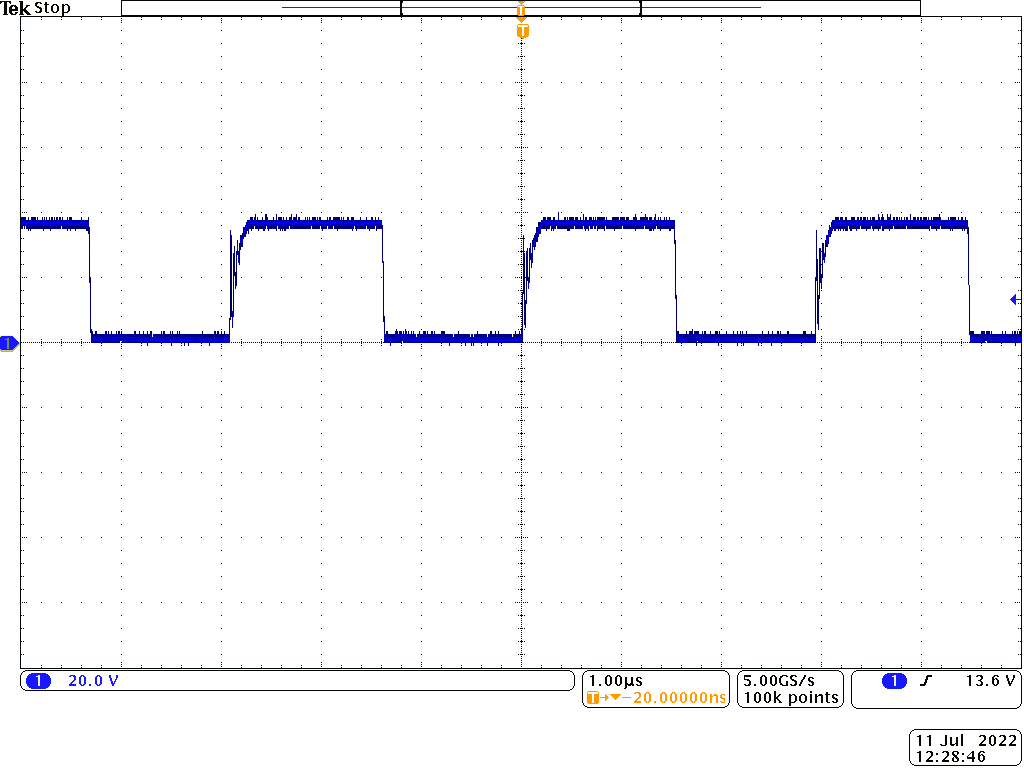
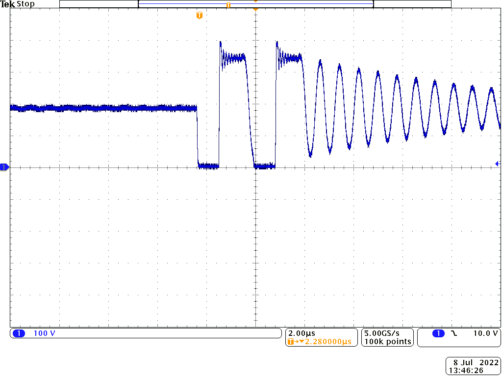
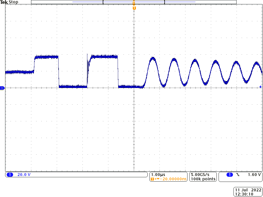
Switching behavior at 132 VAC, 60-Hz input is shown in the following figures. The highest voltage stress on both primary and secondary FETs occurs at highest input voltage and highest output voltage conditions. The voltage stress is highest on the primary FET during Low Power Mode operation of the UCC28782. At this condition, the high-side FET is disabled to conserve power dissipation, resulting in a leakage spike on the primary FET.
 Figure 3-1 Primary FET (U2) Drain-Source Voltage at 20-V
Output and 3-A Load
 Figure 3-3 Secondary FET (Q1) Drain-Source Voltage at
20-V Output and 3-A Load
 Figure 3-2 Primary FET (U2) Drain-Source Voltage at 20-V
Output and 250-mA Load
  Figure 3-4 Secondary FET (Q1) Drain-Source Voltage at
20-V Output and 250-mA Load