SLVSDZ4D February   2018  – February 2020

PRODUCTION DATA.  

  1. Features
  2. Applications
  3. Description
    1.     Simplified Schematic
  4. Revision History
  5. Device Comparison Table
  6. Pin Configuration and Functions
    1.     Pin Functions
    2. 6.1 Recommended Connections for Unused Pins
  7. Specifications
    1. Table 3. Absolute Maximum Ratings
    2. Table 4. ESD Ratings
    3. Table 5. Recommended Operating Conditions
    4. Table 6. Thermal Information
    5. Table 7. Electrical Characteristics
    6. Table 8. SNS Timing Characteristics
    7. Table 9. Switching Characteristics
    8. 7.1      Typical Characteristics
  8. Parameter Measurement Information
  9. Detailed Description
    1. 9.1 Overview
    2. 9.2 Functional Block Diagram
    3. 9.3 Feature Description
      1. 9.3.1 Protection Mechanisms
        1. 9.3.1.1 Thermal Shutdown
        2. 9.3.1.2 Current Limit
          1. 9.3.1.2.1 Current Limit Foldback
          2. 9.3.1.2.2 Programmable Current Limit
          3. 9.3.1.2.3 Undervoltage Lockout (UVLO)
          4. 9.3.1.2.4 VBB During Short-to-Ground
        3. 9.3.1.3 Voltage Transients
          1. 9.3.1.3.1 Load Dump
        4. 9.3.1.4 Driving Inductive Loads
        5. 9.3.1.5 Reverse Battery
        6. 9.3.1.6 Fault Event – Timing Diagrams (Version A/B/C)
      2. 9.3.2 Diagnostic Mechanisms
        1. 9.3.2.1 VOUTx Short-to-Battery and Open-Load
          1. 9.3.2.1.1 Detection With Switch Enabled
          2. 9.3.2.1.2 Detection With Switch Disabled
        2. 9.3.2.2 SNS Output
          1. 9.3.2.2.1 RSNS Value
            1. 9.3.2.2.1.1 High Accuracy Load Current Sense
            2. 9.3.2.2.1.2 SNS Output Filter
        3. 9.3.2.3 Fault Indication and SNS Mux
        4. 9.3.2.4 Resistor Sharing
        5. 9.3.2.5 High-Frequency, Low Duty-Cycle Current Sensing
    4. 9.4 Device Functional Modes
      1. 9.4.1 Off
      2. 9.4.2 Standby
      3. 9.4.3 Diagnostic
      4. 9.4.4 Standby Delay
      5. 9.4.5 Active
      6. 9.4.6 Fault
  10. 10Application and Implementation
    1. 10.1 Application Information
      1. 10.1.1 Ground Protection Network
      2. 10.1.2 Interface With Microcontroller
      3. 10.1.3 I/O Protection
      4. 10.1.4 Inverse Current
      5. 10.1.5 Loss of GND
      6. 10.1.6 Automotive Standards
        1. 10.1.6.1 ISO7637-2
        2. 10.1.6.2 AEC – Q100-012 Short Circuit Reliability
    2. 10.2 Typical Application
      1. 10.2.1 Design Requirements
      2. 10.2.2 Detailed Design Procedure
        1. 10.2.2.1 Thermal Considerations
        2. 10.2.2.2 RILIM Calculation
        3. 10.2.2.3 Diagnostics
          1. 10.2.2.3.1 Selecting the RSNS Value
      3. 10.2.3 Application Curves
  11. 11Power Supply Recommendations
  12. 12Layout
    1. 12.1 Layout Guidelines
    2. 12.2 Layout Example
  13. 13Device and Documentation Support
    1. 13.1 Documentation Support
      1. 13.1.1 Related Documentation
    2. 13.2 Receiving Notification of Documentation Updates
    3. 13.3 Support Resources
    4. 13.4 Trademarks
    5. 13.5 Electrostatic Discharge Caution
    6. 13.6 Glossary
  14. 14Mechanical, Packaging, and Orderable Information

Fault Event – Timing Diagrams (Version A/B/C)

NOTE

All timing diagrams assume that the SELx pins are set to select the relevant channel.

The LATCH, DIA_EN, and ENx pins are controlled by the user. The timing diagrams represent a possible use-case.

Figure 40 shows the immediate current limit switch off and the retry behavior of versions A and B of the device. As shown, the switch will remain latched off until the LATCH pin is low.
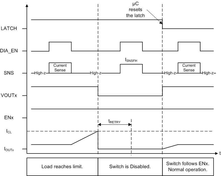
TPS2HB35-Q1 td_01_crrnt_lmt_v_abe_ltchd_behvr_slvsdv7.gifFigure 40. Current Limit – Version A and B - Latched Behavior

Figure 41 shows the immediate current limit switch off behavior of versions A and B. In this example, LATCH is tied to GND; hence, the switch will retry after the fault is cleared and tRETRY has expired.
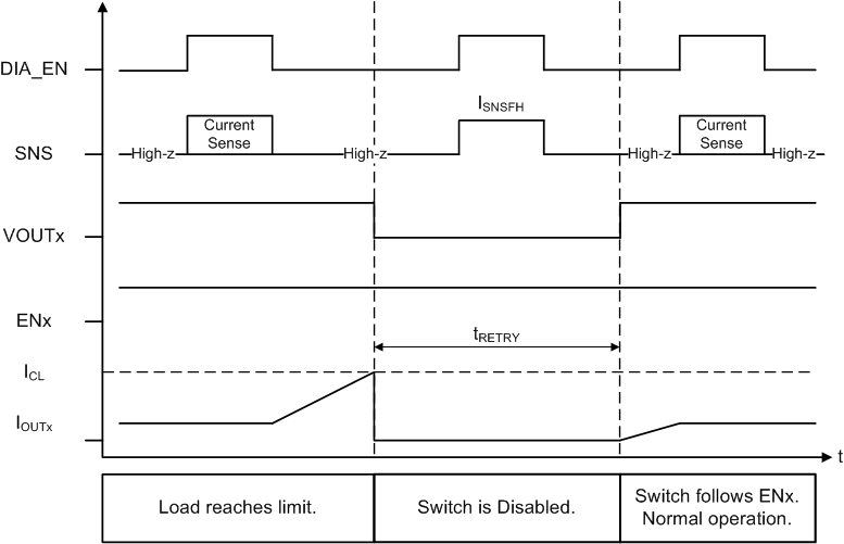
TPS2HB35-Q1 td_02_crrnt_lmt_v_abe_ltchd_zero_slvsdv7.gifFigure 41. Current Limit – Version A and B - LATCH = 0

Figure 42 shows the active current limiting behavior of version C. In version C, the switch will not shutdown until thermal shutdown is reached.
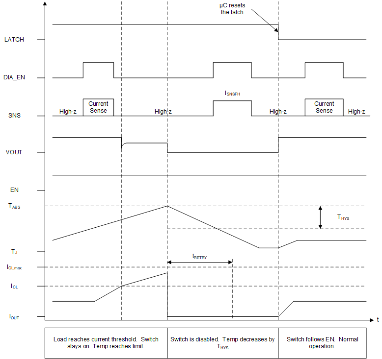
TPS2HB35-Q1 timing-diagrams-td-03_TPS1HBxx.gifFigure 42. Current Limit – Version C - Latched Behavior
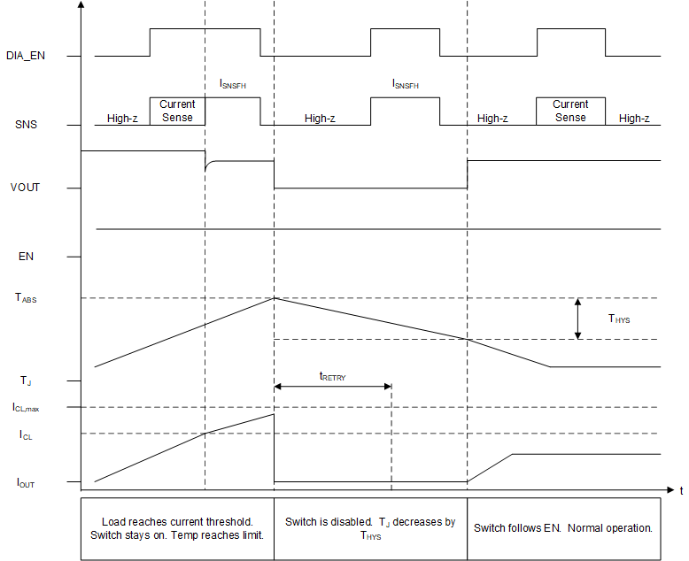
TPS2HB35-Q1 timing-diagrams-td-04_TPS1HBxx.gifFigure 43. Current Limit – Version C - LATCH = 0

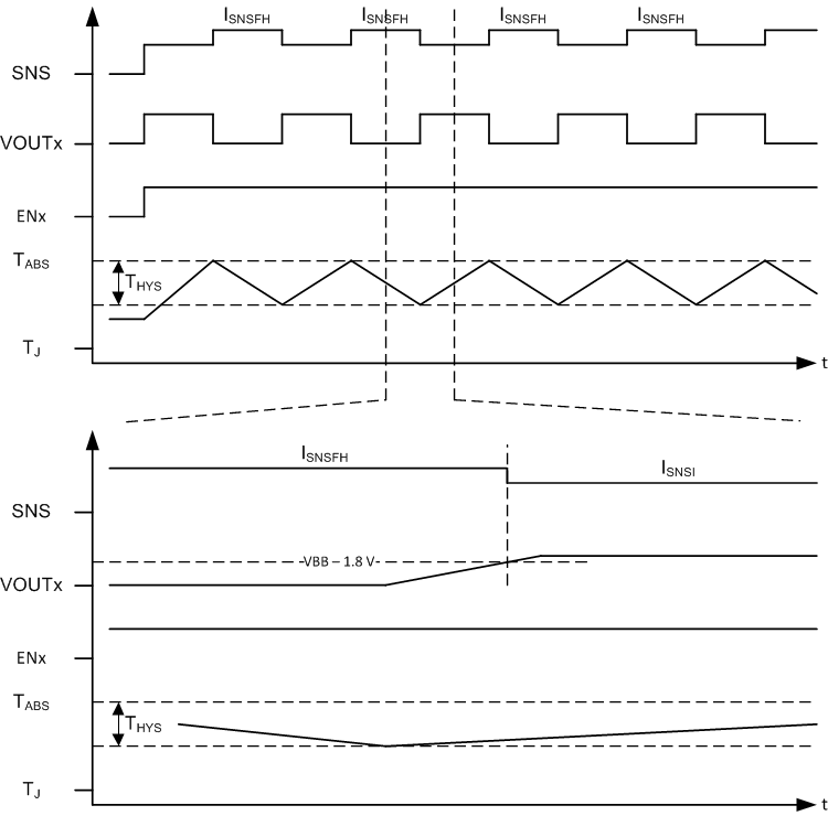
Figure 44 illustrates auto-retry behavior and provides a zoomed-in view of the fault indication during retry. When the switch retries after a shutdown event, the SNS fault indication will remain at the fault state until VOUT has risen to VBB – 1.8 V. Once VOUT has risen, the SNS fault indication is reset and current sensing is available. If there is a short-to-ground and VOUT cannot rise, the SNS fault indication will remain indefinitely.

NOTE

Figure 44 assumes that tRETRY has expired by the time that TJ reaches the hysteresis threshold.

LATCH = 0 V and DIA_EN = 5 V

TPS2HB35-Q1 td_05_fault_indctn_retry_slvsdv7.gifFigure 44. Fault Indication During Retry