SLUUCC4A October 2020 – September 2021 TPS92520-Q1
- Trademarks
- General Texas Instruments High Voltage Evaluation (TI HV EMV) User Safety Guidelines
- 1Description
- 2Performance Specifications
- 3Performance Data and Typical Characteristic Curves
- 4Schematic, PCB Layout, and Bill of Materials
- 5Software
- 6TPS92520EVM-133 Power Up and Operation
- 7Revision History
6 TPS92520EVM-133 Power Up and Operation
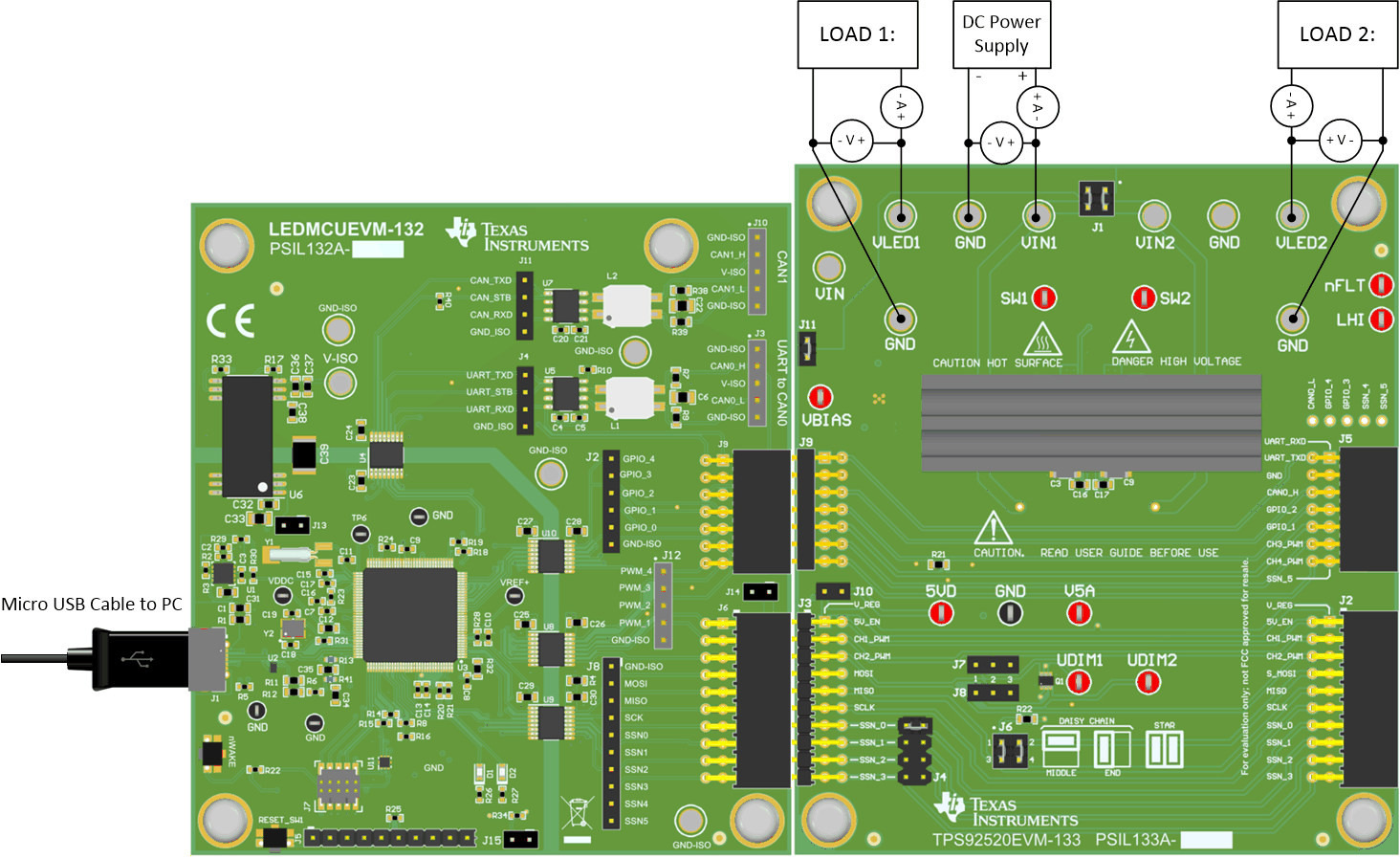
To start the EVM operation, connect the header J9 on TPS92520EVM-133 to the header J9 on the LEDMCUEVM-132, and the header J3 to the header J6, as shown in Figure 6-1.
 Figure 6-1 LEDMCUEVM-132 Connection to TPS92520EVM-133
Apply power (48 V) to the TPS9250EVM-133 board (terminal J1). Connect a resistive or a current sink load such as LEDs or diodes to the output of the EVM (terminal J2). The load must not exceed maximum output current of 1.6 A and the maximum output power of 120 W for two-channel operation. The following steps then provide the necessary setup to enable and turn on the TPS92520EVM-133.
The TPS92520EVM-133 board is setup such that the onboard linear regulator's (U2) input is connected to VIN through J11 and a series zener diode (D3) which reduced the input voltage to the linear's input below 40 V at a VIN of 65 V. The zener helps spread power dissipation between the linear and the zener and protects the linear from being exposed to voltages greater than 40 V.