SLAA870 February   2019 AFE7422 , AFE7444


  1.   Evaluating the frequency hopping capability of the AFE74xx
    1.     Trademarks
    2. 1 Introduction
    3. 2 Phase Coherency vs Phase Continuity
    4. 3 AFE74xx Architecture
      1. 3.1 AFE74xx Receivers: Multiband DDC
      2. 3.2 AFE74xx Transmitters: Multiband DUC
      3. 3.3 Numerically Controlled Oscillator (NCO)
        1. 3.3.1 Programming the NCO frequency
          1. 3.3.1.1 Example: Programming NCO to 1700MHz
        2. 3.3.2 Direct Digital Synthesis (DDS) Mode
    5. 4 Frequency Hopping Methods
      1. 4.1 Maintaining Phase Continuity
        1. 4.1.1 Phase Continuous Hop Time
          1. 4.1.1.1 Serial Peripheral Interface (SPI)
          2. 4.1.1.2 Test Setup
          3. 4.1.1.3 Software Configuration
          4. 4.1.1.4 Test Results
      2. 4.2 Maintaining Phase Coherency
        1. 4.2.1 TX NCO Hopping Using SPI
          1. 4.2.1.1 TX NCO Switch Using SPI Hop Time
            1. 4.2.1.1.1 Software Configuration
            2. 4.2.1.1.2 Test Results
          2. 4.2.1.2 AFE74xx DAC Settling Time
            1. 4.2.1.2.1 Hardware Setup
            2. 4.2.1.2.2 Software Configuration
            3. 4.2.1.2.3 Test Results
        2. 4.2.2 RX NCO Hopping Using the GPIO Pins
          1. 4.2.2.1 Test Setup
          2. 4.2.2.2 Software Configuration
          3. 4.2.2.3 Test Results
    6. 5 NCO Frequency Resolution Versus Hop Time
    7. 6 Fast Frequency Hopping With the Load and Switch
    8. 7 Register Addresses
    9. 8 References

Hardware Setup

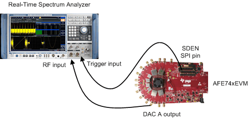
Measuring the settling time for the AFE74xx DACs requires a spectrum analyzer capable of real-time, frequency-domain analysis. As shown inFigure 19, the spectrum analyzer is connected to the DAC A SMA output labeled I_OUTA on the AFE74xxEVM. The SPI clock on the AFE74xxEVM is the trigger source for the spectrum analyzer as the AFE74xx active TX NCO switches from TXNCO0 to TXNCO1.
DAC-settling-time-hardware-setup.gifFigure 19. DAC Settling Time: Hardware Setup