SBAU213A September 2013 – July 2020
7.2 Board Layouts
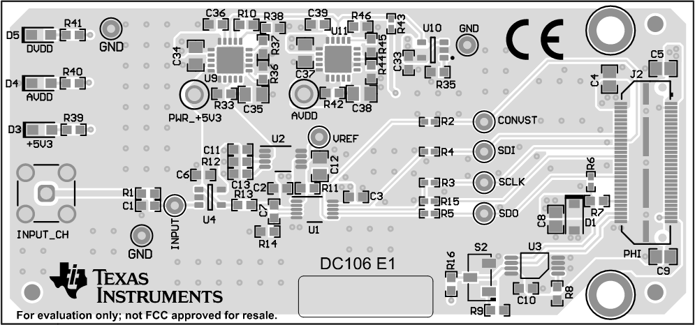
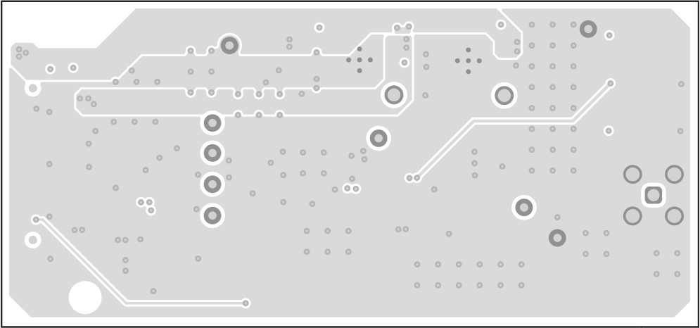
Figure 7-1 and Figure 7-2 show the PCB layouts for the ADS8860EVM.
Note:
Board layouts are not to scale. These figures are intended to show how the board is laid out; they are not intended to be used for manufacturing ADS8860EVM PCBs.
 Figure 7-1 ADS8860EVM PCB: Ground Layer
 Figure 7-2 ADS8860EVM PCB: Bottom Layer (GND)