ZHCSIQ7A august 2018 – december 2021 UCC28951
PRODUCTION DATA
- 1 特性
- 2 应用
- 3 说明
- 4 Revision History
- 5 Pin Configuration and Functions
- 6 Specifications
-
7 Detailed Description
- 7.1 Overview
- 7.2 Functional Block Diagram
- 7.3
Feature Description
- 7.3.1 Start-Up Protection Logic
- 7.3.2 Voltage Reference (VREF)
- 7.3.3 Error Amplifier (EA+, EA–, COMP)
- 7.3.4 Soft-Start and Enable (SS/EN)
- 7.3.5 Light-Load Power Saving Features
- 7.3.6 Adaptive Delay, (Delay Between OUTA and OUTB, OUTC and OUTD (DELAB, DELCD, ADEL))
- 7.3.7 Adaptive Delay (Delay Between OUTA and OUTF, OUTB and OUTE (DELEF, ADELEF)
- 7.3.8 Minimum Pulse (TMIN)
- 7.3.9 Burst Mode
- 7.3.10 Switching Frequency Setting
- 7.3.11 Slope Compensation (RSUM)
- 7.3.12 Dynamic SR ON/OFF Control (DCM Mode)
- 7.3.13 Current Sensing (CS)
- 7.3.14 Cycle-by-Cycle Current Limit Current Protection and Hiccup Mode
- 7.3.15 Synchronization (SYNC)
- 7.3.16 Outputs (OUTA, OUTB, OUTC, OUTD, OUTE, OUTF)
- 7.3.17 Supply Voltage (VDD)
- 7.3.18 Ground (GND)
- 7.4 Device Functional Modes
-
8 Application and Implementation
- 8.1 Application Information
- 8.2
Typical Application
- 8.2.1 Design Requirements
- 8.2.2
Detailed Design Procedure
- 8.2.2.1 Power Loss Budget
- 8.2.2.2 Preliminary Transformer Calculations (T1)
- 8.2.2.3 QA, QB, QC, QD FET Selection
- 8.2.2.4 Selecting LS
- 8.2.2.5 Selecting Diodes DB and DC
- 8.2.2.6 Output Inductor Selection (LOUT)
- 8.2.2.7 Output Capacitance (COUT)
- 8.2.2.8 Select FETs QE and QF
- 8.2.2.9 Input Capacitance (CIN)
- 8.2.2.10 Current Sense Network (CT, RCS, R7, DA)
- 8.2.3 Application Curves
- 9 Power Supply Recommendations
- 10Layout
- 11Device and Documentation Support
8.2.2.3 QA, QB, QC, QD FET Selection
In this design to meet efficiency and voltage requirements 20 A, 650 V, CoolMOS FETs from Infineon are chosen for QA..QD.
The FET drain to source on resistance is:
Equation 46. 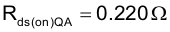
The FET Specified COSS is:
Equation 47. 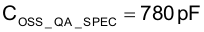
The voltage across drain-to-source (VdsQA) where COSS was measured as a data sheet parameter:
Equation 48. 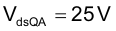
Calculate average Coss [2] using Equation 49:
Equation 49. 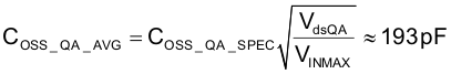
The QA FET gate charge is:
Equation 50. 
The voltage applied to FET gate to activate FET is:
Equation 51. 
Calculate QA losses (PQA) based on Rds(on)QA and gate charge (QAg) using Equation 52:
Equation 52. 
Recalculate the power budget using Equation 53:
Equation 53. 