ZHCSIQ7B August 2018 – October 2024 UCC28950 , UCC28951
PRODUCTION DATA
- 1
- 1 特性
- 2 应用
- 3 说明
- 4 Pin Configuration and Functions
- 5 Specifications
-
6 Detailed Description
- 6.1 Overview
- 6.2 Functional Block Diagram
- 6.3
Feature Description
- 6.3.1 Start-Up Protection Logic
- 6.3.2 Voltage Reference (VREF)
- 6.3.3 Error Amplifier (EA+, EA–, COMP)
- 6.3.4 Soft-Start and Enable (SS/EN)
- 6.3.5 Light-Load Power Saving Features
- 6.3.6 Adaptive Delay, (Delay Between OUTA and OUTB, OUTC and OUTD (DELAB, DELCD, ADEL))
- 6.3.7 Adaptive Delay (Delay Between OUTA and OUTF, OUTB and OUTE (DELEF, ADELEF)
- 6.3.8 Minimum Pulse (TMIN)
- 6.3.9 Burst Mode
- 6.3.10 Switching Frequency Setting
- 6.3.11 Slope Compensation (RSUM)
- 6.3.12 Dynamic SR ON/OFF Control (DCM Mode)
- 6.3.13 Current Sensing (CS)
- 6.3.14 Cycle-by-Cycle Current Limit Current Protection and Hiccup Mode
- 6.3.15 Synchronization (SYNC)
- 6.3.16 Outputs (OUTA, OUTB, OUTC, OUTD, OUTE, OUTF)
- 6.3.17 Supply Voltage (VDD)
- 6.3.18 Ground (GND)
- 6.4 Device Functional Modes
-
7 Application and Implementation
- 7.1 Application Information
- 7.2
Typical Application
- 7.2.1 Design Requirements
- 7.2.2
Detailed Design Procedure
- 7.2.2.1 Power Loss Budget
- 7.2.2.2 Preliminary Transformer Calculations (T1)
- 7.2.2.3 QA, QB, QC, QD FET Selection
- 7.2.2.4 Selecting LS
- 7.2.2.5 Selecting Diodes DB and DC
- 7.2.2.6 Output Inductor Selection (LOUT)
- 7.2.2.7 Output Capacitance (COUT)
- 7.2.2.8 Select FETs QE and QF
- 7.2.2.9 Input Capacitance (CIN)
- 7.2.2.10 Current Sense Network (CT, RCS, R7, DA)
- 7.2.3 Application Curves
- 7.3 Power Supply Recommendations
- 7.4 Layout
- 8 Device and Documentation Support
- 9 Revision History
- 10Mechanical, Packaging, and Orderable Information
6.3.7 Adaptive Delay (Delay Between OUTA and OUTF, OUTB and OUTE (DELEF, ADELEF)
The resistor REF from the DELEF pin to GND along with the resistor divider RAEFHI from CS pin to ADELEF pin and RAEF from ADELEF pin to GND sets equal delays TAFSET and TBESET between outputs OUTA or OUTB going low and related output OUTF or OUTE going low Figure 6-4. The total resistance of this resistor divider should be in the range between 10kΩ and 20kΩ.
 Figure 6-4 Delay
Definitions Between OUTA and OUTF, OUTB and OUTE
Figure 6-4 Delay
Definitions Between OUTA and OUTF, OUTB and OUTEThese delays gradually increase as function of the CS signal from TAFSET1, which is measured at VCS = 0.2V, to TAFSET2, which is measured at VCS = 1.8V. This is opposite to the DELAB and DELCD behavior and this delay is longest (TAFSET2) when the signal at CS pin is maximized and shortest (TAFSET1) when the CS signal is minimized. This approach will reduce the synchronous rectifier MOSFET body diode conduction time over a wide load current range thus improving efficiency. The ratio between the longest and shortest delays is set by the resistor divider RAEFHI and RAEF. If CS and ADELEF are tied, the ratio is maximized. If ADELEF is connected to GND, then the delay is fixed, defined only by resistor REF from DELEF to GND.
The delay time TAFSET is defined by the following Equation 6. Equation 6 also defines the delay time TBESET.
where
- the CS, which is the voltage at pin CS, is in volts
- KEF is a numerical gain factor of CS voltage from 0 to 1
Equation 7 is an empirical approximation of measured data, thus, there is no unit agreement in it. As an example, assume REF = 15kΩ, CS = 1V and KEF = 0.5. Then the TAFSET is going to be 41.7ns. KEF is defined as Equation 7:
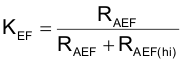
RAEF and RAEFHI define the portion of voltage at pin CS applied to the pin ADELEF (see Figure 7-3). KEF defines how significantly the delay time depends on CS voltage. KEF varies from 0, where ADELEF pin is shorted to ground (RAEF = 0) and the delay does not depend on CS voltage, to 1, where ADELEF is tied to CS (RAEFHI = 0).
The allowed resistor range on DELEF, REF is 13kΩ to 90kΩ.
The plots in Figure 6-5 and Figure 6-6 show delay time settings as function of CS voltage and KEF for two different conditions: REF = 13kΩ (Figure 6-5) and REF = 90kΩ (Figure 6-6)
") Figure 6-5 Delay
Time TAFSET and TBESET (Over CS Voltage and Selected
KEF for REF Equal 13kΩ)
Figure 6-5 Delay
Time TAFSET and TBESET (Over CS Voltage and Selected
KEF for REF Equal 13kΩ)") Figure 6-6 Delay
Time TAFSET and TBESET (Over CS Voltage and Selected
KEF for REF Equal 90kΩ)
Figure 6-6 Delay
Time TAFSET and TBESET (Over CS Voltage and Selected
KEF for REF Equal 90kΩ)