ZHCSIQ7B August 2018 – October 2024 UCC28950 , UCC28951
PRODUCTION DATA
- 1
- 1 特性
- 2 应用
- 3 说明
- 4 Pin Configuration and Functions
- 5 Specifications
-
6 Detailed Description
- 6.1 Overview
- 6.2 Functional Block Diagram
- 6.3
Feature Description
- 6.3.1 Start-Up Protection Logic
- 6.3.2 Voltage Reference (VREF)
- 6.3.3 Error Amplifier (EA+, EA–, COMP)
- 6.3.4 Soft-Start and Enable (SS/EN)
- 6.3.5 Light-Load Power Saving Features
- 6.3.6 Adaptive Delay, (Delay Between OUTA and OUTB, OUTC and OUTD (DELAB, DELCD, ADEL))
- 6.3.7 Adaptive Delay (Delay Between OUTA and OUTF, OUTB and OUTE (DELEF, ADELEF)
- 6.3.8 Minimum Pulse (TMIN)
- 6.3.9 Burst Mode
- 6.3.10 Switching Frequency Setting
- 6.3.11 Slope Compensation (RSUM)
- 6.3.12 Dynamic SR ON/OFF Control (DCM Mode)
- 6.3.13 Current Sensing (CS)
- 6.3.14 Cycle-by-Cycle Current Limit Current Protection and Hiccup Mode
- 6.3.15 Synchronization (SYNC)
- 6.3.16 Outputs (OUTA, OUTB, OUTC, OUTD, OUTE, OUTF)
- 6.3.17 Supply Voltage (VDD)
- 6.3.18 Ground (GND)
- 6.4 Device Functional Modes
-
7 Application and Implementation
- 7.1 Application Information
- 7.2
Typical Application
- 7.2.1 Design Requirements
- 7.2.2
Detailed Design Procedure
- 7.2.2.1 Power Loss Budget
- 7.2.2.2 Preliminary Transformer Calculations (T1)
- 7.2.2.3 QA, QB, QC, QD FET Selection
- 7.2.2.4 Selecting LS
- 7.2.2.5 Selecting Diodes DB and DC
- 7.2.2.6 Output Inductor Selection (LOUT)
- 7.2.2.7 Output Capacitance (COUT)
- 7.2.2.8 Select FETs QE and QF
- 7.2.2.9 Input Capacitance (CIN)
- 7.2.2.10 Current Sense Network (CT, RCS, R7, DA)
- 7.2.3 Application Curves
- 7.3 Power Supply Recommendations
- 7.4 Layout
- 8 Device and Documentation Support
- 9 Revision History
- 10Mechanical, Packaging, and Orderable Information
6.3.8 Minimum Pulse (TMIN)
The resistor RTMIN from the TMIN pin to GND sets a fixed minimum pulse width. This pulse is applied to the transformer and enables ZVS at light load. If the output PWM pulse demanded by the feedback loop is shorter than TMIN, then the controller proceeds to burst mode operation where an even number of TMIN pulses are followed by the off time dictated by the feedback loop. The proper selection of the TMIN duration is dictated by the time it takes to raise sufficient magnetizing current in the power transformer to maintain ZVS. The TMIN pulse is measured from the rising edge of OUTA to the falling edge of OUTD – or from the rising edge of OUTB to the falling edge of OUTC. The minimum pulse TMIN is then defined by Equation 8.

where
- TMIN is in ns
- RTMIN is in kΩ
Various propagation and response time delays in the power circuit modify (usually increase) the pulse width that is measured at the transformer. Select the correct TMIN setting using an iterative process due to the propagation and response time delays in the power circuit.
The minimum allowed resistance on the TMIN pin, RTMIN is 10kΩ.
The related plot is shown in Figure 6-7.
 Figure 6-7 Minimum Time TMIN Over Setting Resistor RTMIN
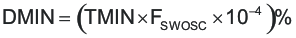
The value of minimum duty cycle DMIN is determined by Equation 9.
where
- FSW(osc) is oscillator frequency in kHz
- TMIN is the minimum pulse in ns
- and DMIN is in percent