ZHCSIQ7B August 2018 – October 2024 UCC28950 , UCC28951
PRODUCTION DATA
- 1
- 1 特性
- 2 应用
- 3 说明
- 4 Pin Configuration and Functions
- 5 Specifications
-
6 Detailed Description
- 6.1 Overview
- 6.2 Functional Block Diagram
- 6.3
Feature Description
- 6.3.1 Start-Up Protection Logic
- 6.3.2 Voltage Reference (VREF)
- 6.3.3 Error Amplifier (EA+, EA–, COMP)
- 6.3.4 Soft-Start and Enable (SS/EN)
- 6.3.5 Light-Load Power Saving Features
- 6.3.6 Adaptive Delay, (Delay Between OUTA and OUTB, OUTC and OUTD (DELAB, DELCD, ADEL))
- 6.3.7 Adaptive Delay (Delay Between OUTA and OUTF, OUTB and OUTE (DELEF, ADELEF)
- 6.3.8 Minimum Pulse (TMIN)
- 6.3.9 Burst Mode
- 6.3.10 Switching Frequency Setting
- 6.3.11 Slope Compensation (RSUM)
- 6.3.12 Dynamic SR ON/OFF Control (DCM Mode)
- 6.3.13 Current Sensing (CS)
- 6.3.14 Cycle-by-Cycle Current Limit Current Protection and Hiccup Mode
- 6.3.15 Synchronization (SYNC)
- 6.3.16 Outputs (OUTA, OUTB, OUTC, OUTD, OUTE, OUTF)
- 6.3.17 Supply Voltage (VDD)
- 6.3.18 Ground (GND)
- 6.4 Device Functional Modes
-
7 Application and Implementation
- 7.1 Application Information
- 7.2
Typical Application
- 7.2.1 Design Requirements
- 7.2.2
Detailed Design Procedure
- 7.2.2.1 Power Loss Budget
- 7.2.2.2 Preliminary Transformer Calculations (T1)
- 7.2.2.3 QA, QB, QC, QD FET Selection
- 7.2.2.4 Selecting LS
- 7.2.2.5 Selecting Diodes DB and DC
- 7.2.2.6 Output Inductor Selection (LOUT)
- 7.2.2.7 Output Capacitance (COUT)
- 7.2.2.8 Select FETs QE and QF
- 7.2.2.9 Input Capacitance (CIN)
- 7.2.2.10 Current Sense Network (CT, RCS, R7, DA)
- 7.2.3 Application Curves
- 7.3 Power Supply Recommendations
- 7.4 Layout
- 8 Device and Documentation Support
- 9 Revision History
- 10Mechanical, Packaging, and Orderable Information
6.3.12 Dynamic SR ON/OFF Control (DCM Mode)
The voltage at the DCM pin provided by the resistor divider RDCMHI between VREF pin and DCM, and RDCM from DCM pin to GND, sets the percentage of 2V current limit threshold for the Current Sense pin, (CS). If the CS pin voltage falls below the DCM pin threshold voltage, then the controller initiates the light load power saving mode, and shuts down the synchronous rectifiers, OUTE and OUTF. If the CS pin voltage is higher than the DCM pin threshold voltage, then the controller runs in CCM mode. Connecting the DCM pin to VREF makes the controller run in DCM mode and shuts both Outputs OUTE and OUTF. Shorting the DCM pin to GND disables the DCM feature and the controller runs in CCM mode under all conditions.
 Figure 6-11 DCM Functional Block
 Figure 6-12 Duty Cycle Change Over Load Current Change
A nominal 20µA switched current source is used to create hysteresis. The current source is active only when the system is in DCM Mode. Otherwise, it is inactive and does not affect the node voltage. Therefore, when in the DCM region, the DCM threshold is the voltage divider plus ΔV explained in Equation 15. When in the CCM region, the threshold is the voltage set by the resistor divider. When the CS pin reaches the threshold set on the DCM pin, the system waits to see two consecutive falling edge PWM cycles before switching from CCM to DCM and vice-versa. The magnitude of the hysteresis is a function of the external resistor divider impedance. The hysteresis can be calculated using Equation 15:
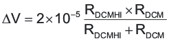
 Figure 6-13 Moving From DCM to CCM Mode
 Figure 6-14 Moving From CCM to DCM Mode
DCM must be used to prevent reverse current in the output inductor which could cause the synchronous FETS to fail.
The controller must switch to DCM mode at a level where the output inductor current is positive. If the output inductor current is negative when the controller switches to DCM mode then the synchronous FETs will see a large VDS spike and may fail.