ZHCSIQ7B August 2018 – October 2024 UCC28950 , UCC28951
PRODUCTION DATA
- 1
- 1 特性
- 2 应用
- 3 说明
- 4 Pin Configuration and Functions
- 5 Specifications
-
6 Detailed Description
- 6.1 Overview
- 6.2 Functional Block Diagram
- 6.3
Feature Description
- 6.3.1 Start-Up Protection Logic
- 6.3.2 Voltage Reference (VREF)
- 6.3.3 Error Amplifier (EA+, EA–, COMP)
- 6.3.4 Soft-Start and Enable (SS/EN)
- 6.3.5 Light-Load Power Saving Features
- 6.3.6 Adaptive Delay, (Delay Between OUTA and OUTB, OUTC and OUTD (DELAB, DELCD, ADEL))
- 6.3.7 Adaptive Delay (Delay Between OUTA and OUTF, OUTB and OUTE (DELEF, ADELEF)
- 6.3.8 Minimum Pulse (TMIN)
- 6.3.9 Burst Mode
- 6.3.10 Switching Frequency Setting
- 6.3.11 Slope Compensation (RSUM)
- 6.3.12 Dynamic SR ON/OFF Control (DCM Mode)
- 6.3.13 Current Sensing (CS)
- 6.3.14 Cycle-by-Cycle Current Limit Current Protection and Hiccup Mode
- 6.3.15 Synchronization (SYNC)
- 6.3.16 Outputs (OUTA, OUTB, OUTC, OUTD, OUTE, OUTF)
- 6.3.17 Supply Voltage (VDD)
- 6.3.18 Ground (GND)
- 6.4 Device Functional Modes
-
7 Application and Implementation
- 7.1 Application Information
- 7.2
Typical Application
- 7.2.1 Design Requirements
- 7.2.2
Detailed Design Procedure
- 7.2.2.1 Power Loss Budget
- 7.2.2.2 Preliminary Transformer Calculations (T1)
- 7.2.2.3 QA, QB, QC, QD FET Selection
- 7.2.2.4 Selecting LS
- 7.2.2.5 Selecting Diodes DB and DC
- 7.2.2.6 Output Inductor Selection (LOUT)
- 7.2.2.7 Output Capacitance (COUT)
- 7.2.2.8 Select FETs QE and QF
- 7.2.2.9 Input Capacitance (CIN)
- 7.2.2.10 Current Sense Network (CT, RCS, R7, DA)
- 7.2.3 Application Curves
- 7.3 Power Supply Recommendations
- 7.4 Layout
- 8 Device and Documentation Support
- 9 Revision History
- 10Mechanical, Packaging, and Orderable Information
6.3.11 Slope Compensation (RSUM)
Slope compensation prevents a sub-harmonic oscillation in the controller during in peak current mode (PCM) control operation or during cycle-by-cycle current limit at duty cycles above 50% (some publications suggest it may happen at D < 50%). Slope compensation in the controller adds an additional ramp signal to the CS signal and is applied to:
- the PWM comparator in the case of peak current mode control
- the input of the cycle-by-cycle comparator
At low duty cycles and light loads, the slope compensation ramp reduces the noise sensitivity during peak current mode control operation.
Placing a resistor from the RSUM pin to ground allows the controller to operate in PCM control. Connecting a resistor from RSUM to VREF switches the controller to voltage mode control (VMC) with the internal PWM ramp. In VMC the resistor at RSUM provides CS signal slope compensation for operation in cycle-by-cycle current limit. That is, in VMC, the slope compensation is applied only to the cycle-by-cycle comparator while in PCM the slope compensation is applied to both the PWM and cycle-by-cycle current limit comparators. The operation logic of the slope compensation circuit is shown in Figure 6-9.
 Figure 6-9 The
Operation Logic of Slope Compensation
Circuit
Figure 6-9 The
Operation Logic of Slope Compensation
CircuitToo much slope compensation reduces the benefits of PCM control. In the case of cycle-by-cycle current limit, the average current limit becomes lower and this might reduce the start-up capability into large output capacitances.
The optimum compensation ramp varies, depending on duty cycle, LOUT and LMAG. A good starting point in selecting the amount of slope compensation is to set the slope compensation ramp to be half the inductor current ramp downslope (inductor current ramp during the off time). The inductor current ramp downslope (as seen at the CS pin input, and neglecting the effects of any filtering at the CS pin) is calculated in Equation 12:
where
- VOUT is the output voltage of the converter
- LOUT is the output inductor value
- a1 is the transformer turns ratio (NP/NS)
- CTRAT is the current transformer ratio (IP/IS, typically 100:1)
Selection of LOUT, a1 and CTRAT are described later in this document. The total slope compensation is 0.5m0. Some of this ramp is due to magnetizing current in the transformer, the rest is added by an appropriately chosen resistor from RSUM to ground.
The slope of the additional ramp, me, added to the CS signal by placing a resistor from RSUM to ground is defined by Equation 13.
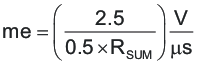
where
- RSUM is in kΩ
- me is in V/μs
If the resistor from the RSUM pin is connected to the VREF pin, then the controller operates in voltage mode control, still having the slope compensation ramp added to the CS signal used for cycle-by-cycle current limit. In this case the slope is defined by Equation 14.
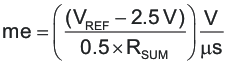
where
- VREF is in volts
- RSUM is in kΩ
- me is in V/μs
These are empirically derived equations without units agreement. As an example, substituting VREF = 5V and RSUM = 40kΩ, yields the result 0.125V/μs. The related plot of me as a function of RSUM is shown in Figure 6-10, Because VREF = 5V, the plots generated from Equation 13 and Equation 14 coincide.
 Figure 6-10 Slope of the Added Ramp Over Resistor
RSUM
Figure 6-10 Slope of the Added Ramp Over Resistor
RSUMThe recommended resistor range for RSUM is 10kΩ to 1MΩ.