ZHCSIQ7A august 2018 – december 2021 UCC28951
PRODUCTION DATA
- 1 特性
- 2 应用
- 3 说明
- 4 Revision History
- 5 Pin Configuration and Functions
- 6 Specifications
-
7 Detailed Description
- 7.1 Overview
- 7.2 Functional Block Diagram
- 7.3
Feature Description
- 7.3.1 Start-Up Protection Logic
- 7.3.2 Voltage Reference (VREF)
- 7.3.3 Error Amplifier (EA+, EA–, COMP)
- 7.3.4 Soft-Start and Enable (SS/EN)
- 7.3.5 Light-Load Power Saving Features
- 7.3.6 Adaptive Delay, (Delay Between OUTA and OUTB, OUTC and OUTD (DELAB, DELCD, ADEL))
- 7.3.7 Adaptive Delay (Delay Between OUTA and OUTF, OUTB and OUTE (DELEF, ADELEF)
- 7.3.8 Minimum Pulse (TMIN)
- 7.3.9 Burst Mode
- 7.3.10 Switching Frequency Setting
- 7.3.11 Slope Compensation (RSUM)
- 7.3.12 Dynamic SR ON/OFF Control (DCM Mode)
- 7.3.13 Current Sensing (CS)
- 7.3.14 Cycle-by-Cycle Current Limit Current Protection and Hiccup Mode
- 7.3.15 Synchronization (SYNC)
- 7.3.16 Outputs (OUTA, OUTB, OUTC, OUTD, OUTE, OUTF)
- 7.3.17 Supply Voltage (VDD)
- 7.3.18 Ground (GND)
- 7.4 Device Functional Modes
-
8 Application and Implementation
- 8.1 Application Information
- 8.2
Typical Application
- 8.2.1 Design Requirements
- 8.2.2
Detailed Design Procedure
- 8.2.2.1 Power Loss Budget
- 8.2.2.2 Preliminary Transformer Calculations (T1)
- 8.2.2.3 QA, QB, QC, QD FET Selection
- 8.2.2.4 Selecting LS
- 8.2.2.5 Selecting Diodes DB and DC
- 8.2.2.6 Output Inductor Selection (LOUT)
- 8.2.2.7 Output Capacitance (COUT)
- 8.2.2.8 Select FETs QE and QF
- 8.2.2.9 Input Capacitance (CIN)
- 8.2.2.10 Current Sense Network (CT, RCS, R7, DA)
- 8.2.3 Application Curves
- 9 Power Supply Recommendations
- 10Layout
- 11Device and Documentation Support
7.3.10 Switching Frequency Setting
Connecting an external resistor RT between the RT pin and VREF pins sets the fixed frequency operation and configures the controller as a leader providing synchronization output pulses at SYNC pin with 0.5 duty cycle and frequency equal to the internal oscillator. Connect an external resistor RT between the RT and GND pins to configure the controller as a follower. When the controller is used in follower mode, connect a 825 kΩ ±5% resistor from the SS pin to the ground pin in parallel with the SS_EN capacitor. The follower controller operates with 90° phase shift relative to the leader converter if their SYNC pins are tied together. The switching frequency of the converter is equal to the frequency of output pulses.
Equation 10 defines the nominal switching frequency of the converter configured as a leader (resistor RT between the RT pin and VREF). On the UCC28951 there is an internal clock oscillator frequency which is twice as that of the controller's output frequency.
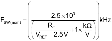
where
- RT is in kΩ
- VREF is in volts
- FSW(nom) is in kHz
This is also an empirical approximation and thus, there is no unit agreement. Assume for example, VREF = 5 V, RT = 65 kΩ. Then the switching frequency FSW(nom) is going to be 92.6 kHz.
Equation 11 defines the nominal switching frequency of converter if the converter configured as a follower and the resistor RT is connected between the RT pin and GND.
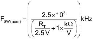
where
- RT is in kΩ
- FSW(nom) is in kHz
Notice that for VREF = 5 V, Equation 10 and Equation 11 yield the same results.
The plot in Figure 7-8 shows how FSW(nom) depends on the resistor RT value when the VREF = 5 V. As it is seen from Equation 10 and Equation 11, the switching frequency FSW(nom) is set to the same value for either leader or follower configuration provided the same resistor value RT is used.
 Over Resistor RT Value") Figure 7-8 Converter Switching Frequency FSW(nom) Over Resistor RT Value
Figure 7-8 Converter Switching Frequency FSW(nom) Over Resistor RT Value