ZHCSKL1A December 2019 – May 2022 TUSS4440
PRODUCTION DATA
- 1 特性
- 2 应用
- 3 说明
- 4 Revision History
- 5 Pin Configuration and Functions
-
6 Specifications
- 6.1 Absolute Maximum Ratings
- 6.2 ESD Ratings
- 6.3 Recommended Operating Conditions
- 6.4 Thermal Information
- 6.5 Power-Up Characteristics
- 6.6 Transducer Drive
- 6.7 Receiver Characteristics
- 6.8 Echo Interrupt Comparator Characteristics
- 6.9 Digital I/O Characteristics
- 6.10 Switching Characteristics
- 6.11 Typical Characteristics
- 7 Detailed Description
- 8 Application and Implementation
- 9 Power Supply Recommendations
- 10Layout
- 11Device and Documentation Support
- 12Mechanical, Packaging, and Orderable Information
7.3.3 Transformer Transducer Drive
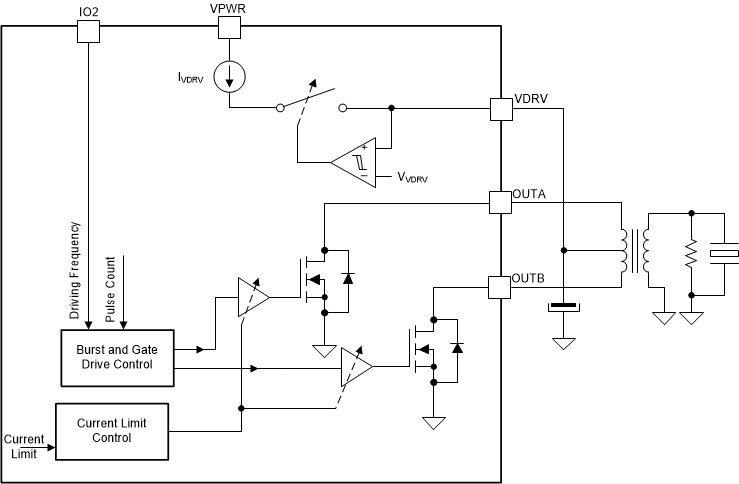
The device provides burst generation by exciting the primary side of a step-up transformer connected at the OUTA / OUTB pins. The VDRV pin is used as the power supply source. Figure 7-5 shows the TUSS4440 device transformer drive block diagram when using a center-tap transformer. The drive stage in the TUSS4440 is realized as two low-side N-Channel power FETs. The current limit control block tries to drive current efficiently into the primary side of the transformer to achieve the maximum swing (set by voltage on the center tap and turn ratio of the transformer) on the secondary side. The secondary side total resistance, turn ratio, and the required peak-to-peak voltage will set the minimum value that will drive the OUTA/OUTB pin for a given set current limit. The current limit block supports multiple current levels selected by the XFMR_DRV_ILIM bits. The voltage on VDRV pin can be set as described in the Section 7.3.1 section.
 Figure 7-5 TUSS4440 Center-Tap transformer drive.
For a center-tap transformer configuration, the TUSS4440 will drive the low-side FETs in an out-of-phase manner. The device also supports a single primary coil transformer configuration where the FETs are driven in-phase. This is done by setting the HALF_BRG_MODE bit. In this mode, the effective current limit remains the same as set in XFMR_DRV_ILIM. Refer to Section 8 for an application diagram and information on how the polarity and state of the OUTA and OUTB pins are defined with respect to the IO1 and IO2 pin states and other register settings.
For a center-tap transformer, the voltage swing on OUTA and OUTB can be as high as 2 × VVDRV. If the center tap of the transformer is connected directly to VPWR, then it must be ensured that the maximum voltage on OUTA and OUTB pins do not go above the absolute maximum limits.