ZHCSKL1A December 2019 – May 2022 TUSS4440
PRODUCTION DATA
- 1 特性
- 2 应用
- 3 说明
- 4 Revision History
- 5 Pin Configuration and Functions
-
6 Specifications
- 6.1 Absolute Maximum Ratings
- 6.2 ESD Ratings
- 6.3 Recommended Operating Conditions
- 6.4 Thermal Information
- 6.5 Power-Up Characteristics
- 6.6 Transducer Drive
- 6.7 Receiver Characteristics
- 6.8 Echo Interrupt Comparator Characteristics
- 6.9 Digital I/O Characteristics
- 6.10 Switching Characteristics
- 6.11 Typical Characteristics
- 7 Detailed Description
- 8 Application and Implementation
- 9 Power Supply Recommendations
- 10Layout
- 11Device and Documentation Support
- 12Mechanical, Packaging, and Orderable Information
7.3.4 Analog Front End
 Figure 7-6 TUSS4440 Analog Front-End Block Diagram
Figure 7-6 shows the analog front-end block diagram that can receive and condition the signals from the transducer during listen mode. The received echo is first amplified with a fixed linear low-noise amplifier, followed by either a bandpass filter or a high-pass filter to remove noise out of the expected signal band. After filtering the signal, the signal is fed into a logarithmic amplifier. The output of the logarithmic amplifier is then buffered to the VOUT pin. In Figure 7-6, every block has the register name associated with it that can be used to configure the signal path. The final equation for the signal path is given by Equation 2:
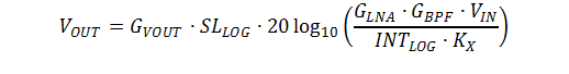
where
- GVOUT is set by the LOGAMP_SLOPE_ADJ bits.
- SLLOG is slope of logarithmic amplifier as specified in the Receiver Characteristics table.
- GLNA is set by the LNA_GAIN bits.
- GBPF is typically 0.9V/V.
- VIN is the input VINP
- INTLOG is logarithmic amplifier intercept specified in the Receiver Characteristics table.
- KX is the log intercept adjustment set by the LOGAMP_INT_ADJ bits.
The bandpass filter is critical for reducing noise to allow utilization of the complete dynamic range of the logarithmic amplifier. The center frequency of the bandpass filter can be configured to be close the transducer frequency which is set by the BPF_HPF_FREQ bits. Table 7-1 shows the nominal values for the BPF center frequency corresponding to the BPF_HPF_FREQ register value. The TUSS4440 supports a wide range of frequencies, therefore a factory trim is used to remove process variation for a particular pre-determined frequency. It is possible that all other frequencies listed in Table 7-1 do not correspond exactly to value of BPF_HPF_FREQ in a factory trim. The user can vary the value of the BPF_HPF_FREQ register around the desired center frequency while actively bursting and observing the VOUT signal. The value with maximum voltage at VOUT pin will the desired setting for the BPF_HPF_FREQ register.
| BPF_HPF_FREQ (HEX) (BPF_FC_TRIM_FRC = 0) | BPF_Fc (KHz) |
|---|---|
| 0x00 | 40.64 |
| 0x01 | 44.05 |
| 0x02 | 45.6 |
| 0x03 | 48.86 |
| 0x04 | 50.58 |
| 0x05 | 52.96 |
| 0x06 | 56.75 |
| 0x07 | 60.11 |
| 0x08 | 62.95 |
| 0x09 | 66.68 |
| 0x0A | 71.44 |
| 0x0B | 74.81 |
| 0x0C | 79.24 |
| 0x0D | 82.03 |
| 0x0E | 86.89 |
| 0x0F | 92.04 |
| 0x10 | 97.49 |
| 0x11 | 103.27 |
| 0x12 | 109.4 |
| 0x13 | 114.54 |
| 0x14 | 121.33 |
| 0x15 | 128.52 |
| 0x16 | 134.58 |
| 0x17 | 142.55 |
| 0x18 | 151.01 |
| 0x19 | 159.94 |
| 0x1A | 167.48 |
| 0x1B | 177.41 |
| 0x1C | 185.77 |
| 0x1D | 196.78 |
| 0x1E | 206.05 |
| 0x1F | 218.26 |
| 0x20 | 228.54 |
| 0x21 | 244.89 |
| 0x22 | 256.43 |
| 0x23 | 271.63 |
| 0x24 | 284.43 |
| 0x25 | 301.28 |
| 0x26 | 319.13 |
| 0x27 | 338.14 |
| 0x28 | 353.97 |
| 0x29 | 374.95 |
| 0x2A | 397.16 |
| 0x2B | 408.17 |
| 0x2C | 420.7 |
| 0x2D | 455.63 |
| 0x2E | 472.03 |
| 0x2F | 500 |
The factory trim can be overridden by setting the BPF_FC_TRIM_FRC bit first and varying the BPF_FC_TRIM bit after. This is useful in two ways:
- If the factory trimmed bandpass filter center frequency is higher than the desired value for BPF_HPF_FREQ = 0x00, or lower than desired value for BPF_HPF_FREQ = 0x2F, then BPF_FC_TRIM can be used to recover the range.
- This setting can also be used to extend the frequency range of the bandpass filter center frequency.
| BPF_HPF_FREQ (hex) + BPF_FC_TRIM (hex) (BPF_FC_TRIM_FRC = 1) | BPF_Fc (KHz) |
|---|---|
| 0x00 + 0x8 | 27.48 |
| 0x00 + 0x9 | 29.44 |
| 0x00 + 0xA | 30.83 |
| 0x00 + 0xB | 31.19 |
| 0x00 + 0xC | 32.65 |
| 0x00 + 0xD | 34.19 |
| 0x00 + 0xE | 35.8 |
| 0x00 + 0xF | 38.81 |
| 0x2F + 0x1 | 523.56 |
| 0x2F + 0x2 | 554.59 |
| 0x2F + 0x3 | 587.45 |
| 0x2F + 0x4 | 622.23 |
| 0x2F + 0x5 | 651.58 |
| 0x2F + 0x6 | 690.19 |
| 0x2F + 0x7 | 731.09 |
- The Q factor of the filter is specified in the Receiver Characteristics table, and can be selected by the BPF_Q_SEL bits.
- The bandpass filter can also be converted into a high-pass filter by setting the BPF_BYPASS bit for transducer frequencies in the range above what is shown in Table 7-1. The corner frequency for high-pass filter is also controlled by the BPF_HPF_FREQ bits.
- BPF_Q_SEL and BPF_FC_TRIM have no effect when BPF_BYPASS = 1.
The logamp provides compression for large signal inputs and amplifies linearly small signal inputs. Logamp simplifies system design to detect varying strengths of echoes that happens because of difference in reflectivity of different types of objects and objects at different distances. It automatically adjusts its gain based on the input signal level. The logamp also demodulates the incoming signal.
The logamp consists of multiple gain stages and range extension stages that are combined to give a logarithmic response. The current consumption of the device can be reduced by turning off the either the first stage, the last stage of the logamp, or both, by setting the LOGAMP_DIS_FIRST and LOGAMP_DIS_LAST bits. Disabling the stages will reduce the input dynamic range on the lower side of the range (see Figure 6-4). The pedestal noise floor will be lower because the gain stages are disabled, but the minimum detectable signal value becomes higher due to the reduced dynamic range. Depending on the received input signal strength, stages can be disabled to get optimum object detection. For very small inputs, all stages should be enabled to get maximum input dynamic range even though the noise floor is higher. Figure 6-6, Figure 6-7, and Figure 6-8 show the effect on the log conformance error when all stages are enabled, when the last stage is disabled, and when both first and last stages are disabled. When stages are disabled, a lower error is obtained with a lower noise floor, but the input dynamic range is reduced.
At the output of the logamp, the user can apply an adjustment to the intercept of the logamp curve. This is denoted by the KX factor in Equation 1. The intercept adjustment is controlled by the LOGAMP_INT_ADJ bits. Table 7-3 shows the nominal values of KX factor corresponding to register values, and Figure 6-14 shows its effect on the transfer function.
| LOGAMP_INT_ADJ | KX |
|---|---|
| 0x00 | 1 |
| 0x01 | 1.155 |
| 0x02 | 1.334 |
| 0x03 | 1.54 |
| 0x04 | 1.778 |
| 0x05 | 2.054 |
| 0x06 | 2.371 |
| 0x07 | 2.738 |
| 0x08 | 1 |
| 0x09 | 0.931 |
| 0x0A | 0.866 |
| 0x0B | 0.806 |
| 0x0C | 0.75 |
| 0x0D | 0.698 |
| 0x0E | 0.649 |
| 0x0F | 0.604 |
The output of the logamp is filtered using a low-pass filter to remove the high-frequency components and provide a sufficient peak hold time for the demodulated envelope signal. The cut-off frequency of the low-pass filter is set by the internal impedance of the FLT pin and the value of an external capacitor connected to the pin. As this filter capacitance (CFLT) suppresses the high frequency fluctuations, it also slows down the response time of the logamp. Higher CFLT capacitance will result in lower peak-to-peak voltage variations at VOUT, and slower rise and fall times for the VOUT voltage to reach its maximum value for a given input signal. A nominal value can be calculated using Equation 3, and must be optimized depending on the application.
The output of the low-pass filter is buffered to the VOUT pin using an internal buffer. The buffer is designed to support an ADC input of a MCU. It is possible to change output dynamic range of the VOUT buffer using the VOUT_SCALE_SEL bit. Once the range is set, the gain of the VOUT buffer can be set by the LOGAMP_SLOPE_ADJ bits. The slope variation of the receiver analog front end is show in Figure 6-13.
Echo interrupt signal is available on the OUT4 pin that goes high when the signal on the VOUT pin crosses a threshold as defined by the ECHO_INT_THR_SEL bits. As long as the VOUT signal is higher than this threshold, the echo interrupt signal is held high. The signal goes low asynchronously when the VOUT signal drops below the programmed threshold. This signal can be used to interrupt a MCU when an object has been detected. The threshold value is also dependent on the setting of the VOUT_SCALE_SEL bit.
A zero-crossing signal is output at the OUT3 pin which can be used to validate the frequency of the received echo signal to provide robustness against interference from other signals. This zero-crossing signal is derived from the raw amplified input signal from a particular stage as it is being demodulated in the logamp block. This function is disabled at device power up. but can be enabled by setting the ZC_CMP_EN bit. When enabled, the ZC_CMP_STG_SEL bits are used to select which logamp gain stage is used to generate the zero crossing signal while the ZC_CMP_HYST bits control the hysteresis of the zero-crossing comparator. The stage selection to see the OUT3 pin toggling depends on the strength of signal received by the logamp and has to be configured depending on the application. For large amplitude of input signal, a lower stage of the logamp should be selected, whereas for lower amplitude signal, a higher stage should be selected. To avoid switching noise generated by the toggling of the zero-crossing comparator when the ZC_EN_ECHO_INT bit is set, the zero-crossing output will be only enabled while the echo interrupt signal is high.