ZHCSK81A September 2019 – October 2020 TPS65296
PRODUCTION DATA
- 1 特性
- 2 应用
- 3 说明
- 4 Revision History
- 5 Pin Configuration and Functions
- 6 Specifications
- 7 Detailed Description
- 8 Application and Implementation
- 9 Power Supply Recommendations
- 10Layout
- 11Device and Documentation Support
- 12Mechanical, Packaging, and Orderable Information
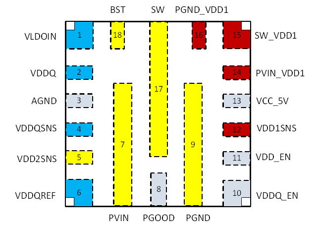
5 Pin Configuration and Functions
 Figure 5-1 18-Pin VQFN RJE Package (Top
View)
Figure 5-1 18-Pin VQFN RJE Package (Top
View)Table 5-1 Pin Functions
| PIN | I/O | DESCRIPTION | |
|---|---|---|---|
| NAME | NO. | ||
| VLDOIN | 1 | P | Power supply input for VDDQ LDO. Connect VDD2 in typical application. |
| VDDQ | 2 | O | VDDQ 1.5-A LDO output. It is recommended to connect to 10-μF or larger capacitance for stability. |
| AGND | 3 | G | Signal ground |
| VDDQSNS | 4 | I | VDDQ output voltage feedback |
| VDD2SNS | 5 | I | VDD2 output voltage feedback |
| VDDQREF | 6 | O | Internal reference for VDDQ. Recommend to connect to 0.22-μF or larger capacitance for stability. |
| PVIN | 7 | P | Input power supply for VDD2 buck |
| PGOOD | 8 | O | Power good signal open-drain output. PGOOD goes high when VDD1 and VDD2 output voltage are within the target range. |
| PGND | 9 | G | Power ground for VDD2 buck |
| VDDQ_EN | 10 | I | VDDQ_EN signal input for VDDQ LDO enable control. For detail control setup, refer to Table 7-1. |
| VDD_EN | 11 | I | VDD_EN signal input for VDD1 buck and VDD2 buck enable control. For detail control setup, refer to Table 7-1. |
| VDD1SNS | 12 | I | VDD1 output voltage feedback |
| VCC_5V | 13 | P | Power supply for VDD1 and VDD2 buck converter control logic circuit |
| PVIN_VDD1 | 14 | P | Input power supply for VDD1 buck |
| SW_VDD1 | 15 | O | VDD1 switching node connection to the inductor and bootstrap capacitor |
| PGND_VDD1 | 16 | G | Power ground for VDD1 buck |
| SW | 17 | O | VDD2 switching node connection to the inductor and bootstrap capacitor |
| BST | 18 | I | High-side MOSFET gate driver bootstrap voltage input for VDD2 buck. Connect a capacitor between the BST pin and the SW pin. |