ZHCSK81A September 2019 – October 2020 TPS65296
PRODUCTION DATA
- 1 特性
- 2 应用
- 3 说明
- 4 Revision History
- 5 Pin Configuration and Functions
- 6 Specifications
- 7 Detailed Description
- 8 Application and Implementation
- 9 Power Supply Recommendations
- 10Layout
- 11Device and Documentation Support
- 12Mechanical, Packaging, and Orderable Information
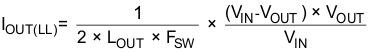
7.3.2 Advanced Eco-mode Control
The VDD1 buck and VDD2 buck are designed with advanced Eco-mode control schemes to maintain high light load efficiency. As the output current decreases from heavy load conditions, the inductor current is also reduced and eventually comes to a point where the rippled valley touches zero level, which is the boundary between continuous conduction and discontinuous conduction modes. The rectifying MOSFET is turned off when the zero inductor current is detected. As the load current further decreases, the converter runs into discontinuous conduction mode. The on-time is kept almost the same as it was in the continuous conduction mode, so that it takes longer time to discharge the output capacitor with smaller load current to the level of the reference voltage. This makes the switching frequency lower, proportional to the load current, and keeps the light load efficiency high. The light load current where the transition to Eco-mode operation happens (IOUT(LL)) can be calculated from Equation 2.
After identifying the application requirements, design the output inductance (LOUT) so that the inductor peak-to-peak ripple current is approximately between 20% and 30% of the IOUT(max) (peak current in the application). It is also important to size the inductor properly so that the valley current does not hit the negative low-side current limit.