ZHCSK81A September   2019  – October 2020 TPS65296

PRODUCTION DATA  

  1. 特性
  2. 应用
  3. 说明
  4. Revision History
  5. Pin Configuration and Functions
  6. Specifications
    1. 6.1 Absolute Maximum Ratings
    2. 6.2 ESD Ratings
    3. 6.3 Recommended Operating Conditions
    4. 6.4 Thermal Information
    5. 6.5 Electrical Characteristics
    6. 6.6 Typical Characteristics
  7. Detailed Description
    1. 7.1 Overview
    2. 7.2 Functional Block Diagram
    3. 7.3 Feature Description
      1. 7.3.1 PWM Operation and D-CAP3 Control
      2. 7.3.2 Advanced Eco-mode Control
      3. 7.3.3 Soft Start and Prebiased Soft Start
      4. 7.3.4 Power Good
      5. 7.3.5 Overcurrent Protection and Undervoltage Protection
      6. 7.3.6 Overvoltage Protection
      7. 7.3.7 UVLO Protection
      8. 7.3.8 Output Voltage Discharge
      9. 7.3.9 Thermal Shutdown
    4. 7.4 Device Functional Modes
      1. 7.4.1 Light Load Operation for VDD1 Buck and VDD2 Buck
      2. 7.4.2 Output State Control
      3. 7.4.3 Output Sequence Control
  8. Application and Implementation
    1. 8.1 Application Information
    2. 8.2 Typical Application
      1. 8.2.1 Design Requirements
      2. 8.2.2 Detailed Design Procedure
        1. 8.2.2.1 External Component Selection
          1. 8.2.2.1.1 Inductor Selection
          2. 8.2.2.1.2 Output Capacitor Selection
          3. 8.2.2.1.3 Input Capacitor Selection
          4. 8.2.2.1.4 Bootstrap Capacitor and Resistor Selection
      3. 8.2.3 Application Curves
  9. Power Supply Recommendations
  10. 10Layout
    1. 10.1 Layout Guidelines
    2. 10.2 Layout Example
  11. 11Device and Documentation Support
    1. 11.1 Device Support
      1. 11.1.1 Third-Party Products Disclaimer
    2. 11.2 Support Resources
    3. 11.3 Receiving Notification of Documentation Updates
    4. 11.4 Trademarks
    5. 11.5 Electrostatic Discharge Caution
    6. 11.6 Glossary
  12. 12Mechanical, Packaging, and Orderable Information

封装选项

机械数据 (封装 | 引脚)
散热焊盘机械数据 (封装 | 引脚)
订购信息
Input Capacitor Selection

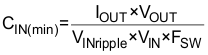
The TPS65296 requires input decoupling capacitors on both power supply input PVIN and PVIN_VDD1, and the bulk capacitors are needed depending on the application. The minimum input capacitance required is given in Equation 5.

Equation 5. GUID-71780B95-389B-45E5-B6CF-C936490D3D49-low.gif

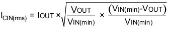
TI recommends using a high-quality X5R or X7R input decoupling capacitors of 30 µF on the VDD2 buck input voltage pin PVIN, and 10 µF on the VDD1 buck input voltage pin PVIN_VDD1. The voltage rating on the input capacitor must be greater than the maximum input voltage. The capacitor must also have a ripple current rating greater than the maximum input current ripple of the application. The input ripple current is calculated by Equation 6:

Equation 6. GUID-7499CF2A-DAB9-43B5-B11F-B7B5DF13BBAA-low.gif

An additional 0.1-µF capacitor from PVIN to ground and from PVIN_VDD1 to ground is optional to provide additional high frequency filtering. One ceramic capacitor of 10 µF is recommended for the decoupling capacitor on VLDOIN pin for providing stable power on VDDQ LDO block. A 1-µF ceramic capacitor is needed for the decoupling capacitor on VCC_5V input.