ZHCSPP3 July 2022 TPS563300
PRODUCTION DATA
- 1 特性
- 2 应用
- 3 说明
- 4 Revision History
- 5 Pin Configuration and Functions
- 6 Specifications
-
7 Detailed Description
- 7.1 Overview
- 7.2 Functional Block Diagram
- 7.3
Feature Description
- 7.3.1 Fixed Frequency Peak Current Mode
- 7.3.2 Pulse Frequency Modulation
- 7.3.3 Voltage Reference
- 7.3.4 Output Voltage Setting
- 7.3.5 Enable and Adjusting Undervoltage Lockout
- 7.3.6 Minimum On Time, Minimum Off Time, and Frequency Foldback
- 7.3.7 Frequency Spread Spectrum
- 7.3.8 Overvoltage Protection
- 7.3.9 Overcurrent and Undervoltage Protection
- 7.3.10 Thermal Shutdown
- 7.4 Device Functional Modes
-
8 Application and Implementation
- 8.1 Application Information
- 8.2
Typical Application
- 8.2.1 Design Requirements
- 8.2.2
Detailed Design Procedure
- 8.2.2.1 Custom Design With WEBENCH® Tools
- 8.2.2.2 Output Voltage Resistors Selection
- 8.2.2.3 Bootstrap Capacitor Selection
- 8.2.2.4 Undervoltage Lockout Set Point
- 8.2.2.5 Output Inductor Selection
- 8.2.2.6 Output Capacitor Selection
- 8.2.2.7 Input Capacitor Selection
- 8.2.2.8 Feedforward Capacitor CFF Selection
- 8.2.2.9 Maximum Ambient Temperature
- 8.2.3 Application Curves
- 8.3 Best Design Practices
- 8.4 Power Supply Recommendations
- 8.5 Layout
- 9 Device and Documentation Support
- 10Mechanical, Packaging, and Orderable Information
8.4 Power Supply Recommendations
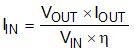
The devices are designed to operate from an input voltage supply range between 3.8 V and 30 V. This input supply must be well regulated and compatible with the limits found in the specifications of this data sheet. In addition, the input supply must be capable of delivering the required input current to the loaded converter. The average input current can be estimated with Equation 23.
where
- ŋ = efficiency
If the converter is connected to the input supply through long wires or PCB traces, special care is required to achieve good performance. The parasitic inductance and resistance of the input cables can have an adverse effect on the operation of the converter. The parasitic inductance, in combination with the low-ESR, ceramic input capacitors, can form an under-damped resonant circuit, resulting in overvoltage transients at the input to the converter. The parasitic resistance can cause the voltage at the VIN pin to dip whenever a load transient is applied to the output. If the application is operating close to the minimum input voltage, this dip can cause the converter to momentarily shutdown and reset. The best way to solve these kind of issues is to reduce the distance from the input supply to the converter and use an aluminum or tantalum input capacitor in parallel with the ceramics. The moderate ESR of these types of capacitors help damp the input resonant circuit and reduce any overshoots. A value in the range of 20 μF to 100 μF is usually sufficient to provide input damping and help hold the input voltage steady during large load transients.
It is recommended that the input supply must not be allowed to fall below the output voltage by more than 0.3 V. Under such conditions, the output capacitors discharges through the body diode of the high-side power MOSFET. The resulting current can cause unpredictable behavior, and in extreme cases, possible device damage. If the application allows for this possibility, then use a Schottky diode from VIN to VOUT to provide a path around the converter for this current.
In some cases, a transient voltage suppressor (TVS) is used on the input of converters. One class of this device has a snap-back characteristic (thyristor type). The use of a device with this type of characteristic is not recommended. When the TVS fires, the clamping voltage falls to a very low value. If this voltage is less than the output voltage of the converter, the output capacitors discharges through the device, as mentioned above.
Sometimes, for other system considerations, an input filter is used in front of the converter. This can lead to instability as well as some of the effects mentioned above, unless it is designed carefully. The AN-2162 Simple Success with Conducted EMI from DCDC Converters User's Guide provides helpful suggestions when designing an input filter for any switching converter.