ZHCSPP3 July 2022 TPS563300
PRODUCTION DATA
- 1 特性
- 2 应用
- 3 说明
- 4 Revision History
- 5 Pin Configuration and Functions
- 6 Specifications
-
7 Detailed Description
- 7.1 Overview
- 7.2 Functional Block Diagram
- 7.3
Feature Description
- 7.3.1 Fixed Frequency Peak Current Mode
- 7.3.2 Pulse Frequency Modulation
- 7.3.3 Voltage Reference
- 7.3.4 Output Voltage Setting
- 7.3.5 Enable and Adjusting Undervoltage Lockout
- 7.3.6 Minimum On Time, Minimum Off Time, and Frequency Foldback
- 7.3.7 Frequency Spread Spectrum
- 7.3.8 Overvoltage Protection
- 7.3.9 Overcurrent and Undervoltage Protection
- 7.3.10 Thermal Shutdown
- 7.4 Device Functional Modes
-
8 Application and Implementation
- 8.1 Application Information
- 8.2
Typical Application
- 8.2.1 Design Requirements
- 8.2.2
Detailed Design Procedure
- 8.2.2.1 Custom Design With WEBENCH® Tools
- 8.2.2.2 Output Voltage Resistors Selection
- 8.2.2.3 Bootstrap Capacitor Selection
- 8.2.2.4 Undervoltage Lockout Set Point
- 8.2.2.5 Output Inductor Selection
- 8.2.2.6 Output Capacitor Selection
- 8.2.2.7 Input Capacitor Selection
- 8.2.2.8 Feedforward Capacitor CFF Selection
- 8.2.2.9 Maximum Ambient Temperature
- 8.2.3 Application Curves
- 8.3 Best Design Practices
- 8.4 Power Supply Recommendations
- 8.5 Layout
- 9 Device and Documentation Support
- 10Mechanical, Packaging, and Orderable Information
7.3.4 Output Voltage Setting
A precision 0.8-V internal reference voltage, VREF, is used to maintain a tightly regulated output voltage over the entire operating temperature range. The output voltage is set by a resistor divider from the output voltage to the FB pin. TI recommends using 1% tolerance resistors with a low temperature coefficient for the FB divider. Select the bottom-side resistor, RFBB, for the desired divider current and use Equation 1 to calculate the top-side resistor, RFBT. Lower RFBB increases the divider current and reduces efficiency at very light load. Larger RFBB makes the FB voltage more susceptible to noise, so the larger RFBB value requires more carefully designed feedback path on the PCB. Setting RFBB = 10 kΩ and RFBT in the range of 10 kΩ to 300 kΩ is recommended for most applications.
The tolerance and temperature variation of the resistor dividers affect the output voltage regulation.
 Figure 7-2 Output Voltage Setting
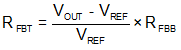
where
- VREF is 0.8 V.
- RFBB is 10 kΩ (recommended).