ZHCSPP3 July 2022 TPS563300
PRODUCTION DATA
- 1 特性
- 2 应用
- 3 说明
- 4 Revision History
- 5 Pin Configuration and Functions
- 6 Specifications
-
7 Detailed Description
- 7.1 Overview
- 7.2 Functional Block Diagram
- 7.3
Feature Description
- 7.3.1 Fixed Frequency Peak Current Mode
- 7.3.2 Pulse Frequency Modulation
- 7.3.3 Voltage Reference
- 7.3.4 Output Voltage Setting
- 7.3.5 Enable and Adjusting Undervoltage Lockout
- 7.3.6 Minimum On Time, Minimum Off Time, and Frequency Foldback
- 7.3.7 Frequency Spread Spectrum
- 7.3.8 Overvoltage Protection
- 7.3.9 Overcurrent and Undervoltage Protection
- 7.3.10 Thermal Shutdown
- 7.4 Device Functional Modes
-
8 Application and Implementation
- 8.1 Application Information
- 8.2
Typical Application
- 8.2.1 Design Requirements
- 8.2.2
Detailed Design Procedure
- 8.2.2.1 Custom Design With WEBENCH® Tools
- 8.2.2.2 Output Voltage Resistors Selection
- 8.2.2.3 Bootstrap Capacitor Selection
- 8.2.2.4 Undervoltage Lockout Set Point
- 8.2.2.5 Output Inductor Selection
- 8.2.2.6 Output Capacitor Selection
- 8.2.2.7 Input Capacitor Selection
- 8.2.2.8 Feedforward Capacitor CFF Selection
- 8.2.2.9 Maximum Ambient Temperature
- 8.2.3 Application Curves
- 8.3 Best Design Practices
- 8.4 Power Supply Recommendations
- 8.5 Layout
- 9 Device and Documentation Support
- 10Mechanical, Packaging, and Orderable Information
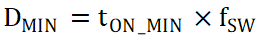
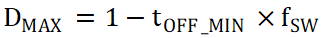
7.3.6 Minimum On Time, Minimum Off Time, and Frequency Foldback
Minimum on time, tON_MIN, is the smallest duration of time that the high-side switch can be on. tON_MIN is typically 70 ns in the TPS563300. Minimum off time, tOFF_MIN, is the smallest duration that the high-side switch can be off. tOFF_MIN is typically 140 ns. In CCM operation, tON_MIN and tOFF_MIN limit the voltage conversion range without switching frequency foldback.
The minimum duty cycle without frequency foldback allowed is:
The maximum duty cycle without frequency foldback allowed is:
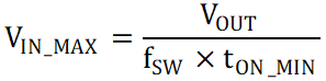
Given a required output voltage, the maximum VIN without frequency foldback is:
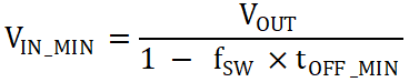
The minimum VIN without frequency foldback is:
In TPS563300, a frequency foldback scheme is employed once tON_MIN or tOFF_MIN is triggered, which can extend the maximum duty cycle or lower the minimum duty cycle.
The on time decreases while VIN voltage increases. Once the on time decreases to tON_MIN, the switching frequency starts to decrease while VIN continues to go up, which lowers the duty cycle further to keep VOUT in regulation according to Equation 5.
The frequency foldback scheme also works once larger duty cycle is needed under low VIN condition. The frequency decreases once the device hits its tOFF_MIN, which extends the maximum duty cycle according to Equation 6. Wide range of frequency foldback allows the TPS563300 output voltage to stay in regulation with a much lower supply voltage VIN, which allows a lower effective dropout.
With frequency foldback, VIN_MAX is raised, and VIN_MIN is lowered by decreased fSW.