ZHCSPP3 July 2022 TPS563300
PRODUCTION DATA
- 1 特性
- 2 应用
- 3 说明
- 4 Revision History
- 5 Pin Configuration and Functions
- 6 Specifications
-
7 Detailed Description
- 7.1 Overview
- 7.2 Functional Block Diagram
- 7.3
Feature Description
- 7.3.1 Fixed Frequency Peak Current Mode
- 7.3.2 Pulse Frequency Modulation
- 7.3.3 Voltage Reference
- 7.3.4 Output Voltage Setting
- 7.3.5 Enable and Adjusting Undervoltage Lockout
- 7.3.6 Minimum On Time, Minimum Off Time, and Frequency Foldback
- 7.3.7 Frequency Spread Spectrum
- 7.3.8 Overvoltage Protection
- 7.3.9 Overcurrent and Undervoltage Protection
- 7.3.10 Thermal Shutdown
- 7.4 Device Functional Modes
-
8 Application and Implementation
- 8.1 Application Information
- 8.2
Typical Application
- 8.2.1 Design Requirements
- 8.2.2
Detailed Design Procedure
- 8.2.2.1 Custom Design With WEBENCH® Tools
- 8.2.2.2 Output Voltage Resistors Selection
- 8.2.2.3 Bootstrap Capacitor Selection
- 8.2.2.4 Undervoltage Lockout Set Point
- 8.2.2.5 Output Inductor Selection
- 8.2.2.6 Output Capacitor Selection
- 8.2.2.7 Input Capacitor Selection
- 8.2.2.8 Feedforward Capacitor CFF Selection
- 8.2.2.9 Maximum Ambient Temperature
- 8.2.3 Application Curves
- 8.3 Best Design Practices
- 8.4 Power Supply Recommendations
- 8.5 Layout
- 9 Device and Documentation Support
- 10Mechanical, Packaging, and Orderable Information
8.5.1 Layout Guidelines
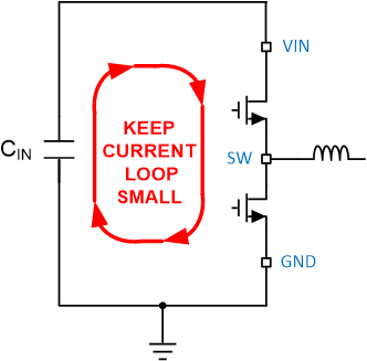
The PCB layout of any DC/DC converter is critical to the optimal performance of the design. Bad PCB layout can disrupt the operation of a good schematic design. Even if the converter regulates correctly, bad PCB layout can mean the difference between a robust design and one that cannot be mass produced. Furthermore, the EMI performance of the converter is dependent on the PCB layout to a great extent. In a buck converter, the most critical PCB feature is the loop formed by the input capacitors and power ground, as shown in Figure 8-22. This loop carries large transient currents that can cause large transient voltages when reacting with the trace inductance. These unwanted transient voltages disrupt the proper operation of the converter. Because of this, the traces in this loop must be wide and short, and the loop area as small as possible to reduce the parasitic inductance.
TI recommends a 2-layer board with 2-oz copper thickness of top and bottom layer, and proper layout provides low current conduction impedance, proper shielding, and lower thermal resistance. Figure 8-23 and Figure 8-24 show the recommended layouts for the critical components of the TPS563300.
- Place the inductor, input and output capacitors, and the IC on the same layer.
- Place the input and output capacitors as close as possible to the IC. The VIN and GND traces must be as wide as possible and provide sufficient vias on them to minimize trace impedance. The wide areas are also of advantage from the view point of heat dissipation.
- Place a 0.1-µF ceramic decoupling capacitor or capacitors as close as possible to VIN and GND, which is key to EMI reduction.
- Keep the SW trace as physically short and wide as practical to minimize radiated emissions.
- Place a BST capacitor and resistor close to BST pin and SW node. > 10-mil width trace is recommended to reduce the parasitic inductance.
- Place the feedback divider as close as possible to the FB pin. > 10-mil width trace is recommended for heat dissipation. Connect a separate VOUT trace to the upper feedback resistor. Place the voltage feedback loop away from the high-voltage switching trace. The feedback loop preferably has ground shield.
 Figure 8-22 Current Loop With Fast Edges