ZHCSPP3 July 2022 TPS563300
PRODUCTION DATA
- 1 特性
- 2 应用
- 3 说明
- 4 Revision History
- 5 Pin Configuration and Functions
- 6 Specifications
-
7 Detailed Description
- 7.1 Overview
- 7.2 Functional Block Diagram
- 7.3
Feature Description
- 7.3.1 Fixed Frequency Peak Current Mode
- 7.3.2 Pulse Frequency Modulation
- 7.3.3 Voltage Reference
- 7.3.4 Output Voltage Setting
- 7.3.5 Enable and Adjusting Undervoltage Lockout
- 7.3.6 Minimum On Time, Minimum Off Time, and Frequency Foldback
- 7.3.7 Frequency Spread Spectrum
- 7.3.8 Overvoltage Protection
- 7.3.9 Overcurrent and Undervoltage Protection
- 7.3.10 Thermal Shutdown
- 7.4 Device Functional Modes
-
8 Application and Implementation
- 8.1 Application Information
- 8.2
Typical Application
- 8.2.1 Design Requirements
- 8.2.2
Detailed Design Procedure
- 8.2.2.1 Custom Design With WEBENCH® Tools
- 8.2.2.2 Output Voltage Resistors Selection
- 8.2.2.3 Bootstrap Capacitor Selection
- 8.2.2.4 Undervoltage Lockout Set Point
- 8.2.2.5 Output Inductor Selection
- 8.2.2.6 Output Capacitor Selection
- 8.2.2.7 Input Capacitor Selection
- 8.2.2.8 Feedforward Capacitor CFF Selection
- 8.2.2.9 Maximum Ambient Temperature
- 8.2.3 Application Curves
- 8.3 Best Design Practices
- 8.4 Power Supply Recommendations
- 8.5 Layout
- 9 Device and Documentation Support
- 10Mechanical, Packaging, and Orderable Information
8.2.2.5 Output Inductor Selection
The most critical parameters for the inductor are the inductance, saturation current, and the RMS current. The inductance is based on the desired peak-to-peak ripple current, ΔiL, which can be calculated by Equation 13.
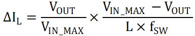
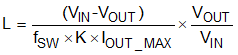
Usually, define K coefficient represents the amount of inductor ripple current relative to the maximum output current of the device, a reasonable value of K must be 20% to 60%, experience shows that the best value of K is 40%. Since the ripple current increases with the input voltage, the maximum input voltage is always used to calculate the minimum inductance L. Use Equation 14 to calculate the minimum value of the output inductor.
where
- K is the ripple ratio of the inductor current (ΔIL / IOUT_MAX).
In general, it is preferable to choose lower inductance in switching power supplies, because it usually corresponds to faster transient response, smaller DCR, and reduced size for more compact designs. Too low of an inductance can generate too large of an inductor current ripple such that overcurrent protection at the full load can be falsely triggered. Too low of an inductance also generates more inductor core loss since the current ripple is larger. Larger inductor current ripple also implies larger output voltage ripple with the same output capacitors.
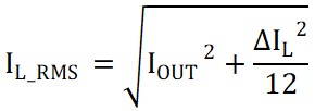
After inductance L is determined, the maximum inductor peak current and RMS current can be calculated by Equation 15 and Equation 16.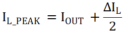
Ideally, the saturation current rating of the inductor is at least as large as the high-side switch current limit, IHS_LIMIT (see Section 6.5), which ensures that the inductor does not saturate even during a short circuit on the output. When the inductor core material saturates, the inductance falls to a very low value, causing the inductor current to rise very rapidly. Although the valley current limit, ILS_LIMIT, is designed to reduce the risk of current runaway, a saturated inductor can cause the current to rise to high values very rapidly, this can lead to component damage, so do not allow the inductor to saturate. In any case, the inductor saturation current must not be less than the maximum peak inductor current at full load.
For this design example, choose the following values:
- K = 0.4
- VIN_MAX = 30 V
- fSW = 500 kHz
- IOUT_MAX = 3 A
The inductor value is calculated to be 6.94 μH. Choose the nearest standard value of 6.8 μH. This gives a new K value of 0.408. The max IHS_LIMIT is 5.8 A, the calculated peak current is 3.61 A, and the calculated RMS current is 3.02 A. The chosen inductor is a Würth Elektronik, 74439346068, 6.8 μH, which has a saturation current rating of 10 A and a RMS current rating of 6.5 A.
The maximum inductance is limited by the minimum current ripple required for the peak current mode control to perform correctly. To avoid subharmonic oscillation, as a rule-of-thumb, the minimum inductor ripple current must be no less than about 10% of the device maximum rated current (3 A) under nominal conditions.