ZHCSPP3 July 2022 TPS563300
PRODUCTION DATA
- 1 特性
- 2 应用
- 3 说明
- 4 Revision History
- 5 Pin Configuration and Functions
- 6 Specifications
-
7 Detailed Description
- 7.1 Overview
- 7.2 Functional Block Diagram
- 7.3
Feature Description
- 7.3.1 Fixed Frequency Peak Current Mode
- 7.3.2 Pulse Frequency Modulation
- 7.3.3 Voltage Reference
- 7.3.4 Output Voltage Setting
- 7.3.5 Enable and Adjusting Undervoltage Lockout
- 7.3.6 Minimum On Time, Minimum Off Time, and Frequency Foldback
- 7.3.7 Frequency Spread Spectrum
- 7.3.8 Overvoltage Protection
- 7.3.9 Overcurrent and Undervoltage Protection
- 7.3.10 Thermal Shutdown
- 7.4 Device Functional Modes
-
8 Application and Implementation
- 8.1 Application Information
- 8.2
Typical Application
- 8.2.1 Design Requirements
- 8.2.2
Detailed Design Procedure
- 8.2.2.1 Custom Design With WEBENCH® Tools
- 8.2.2.2 Output Voltage Resistors Selection
- 8.2.2.3 Bootstrap Capacitor Selection
- 8.2.2.4 Undervoltage Lockout Set Point
- 8.2.2.5 Output Inductor Selection
- 8.2.2.6 Output Capacitor Selection
- 8.2.2.7 Input Capacitor Selection
- 8.2.2.8 Feedforward Capacitor CFF Selection
- 8.2.2.9 Maximum Ambient Temperature
- 8.2.3 Application Curves
- 8.3 Best Design Practices
- 8.4 Power Supply Recommendations
- 8.5 Layout
- 9 Device and Documentation Support
- 10Mechanical, Packaging, and Orderable Information
7.3.5 Enable and Adjusting Undervoltage Lockout
The EN pin provides electrical ON and OFF control of the device. When the EN pin voltage exceeds the enable threshold voltage, VEN_RISE, the TPS563300 begins operation. If the EN pin voltage is pulled below the disable threshold voltage, VEN_FALL, the converter stops switching and enters shutdown mode.
The EN pin has an internal pullup current source, which allows the user to float the EN pin to enable the device. If an application requires control of the EN pin, use open-drain or open-collector or GPIO output logic to interface with the pin.
The TPS563300 implements internal undervoltage-lockout (UVLO) circuitry on the VIN pin. The device is disabled when the VIN pin voltage falls below the internal VIN_UVLO threshold. The internal VIN_UVLO threshold has a hysteresis of typical 300 mV. If an application requires a higher UVLO threshold on the VIN pin, the EN pin can be configured as shown in Figure 7-3. When using the external UVLO function, setting the hysteresis at a value greater than 500 mV is recommended.
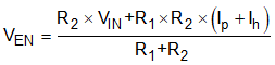
The EN pin has a small pullup current, Ip, which sets the default state of the EN pin to enable when no external components are connected. The pullup hysteresis current, Ih, is used to control the hysteresis voltage for the UVLO function when the EN pin voltage crosses the enable threshold. Use Equation 2 and Equation 3 to calculate the values of R1 and R2 for a specified UVLO threshold. Once R1 and R2 are settled down, the VEN can be calculated by Equation 4, which must be lower than 5.5 V with max VIN.
 Figure 7-3 Adjustable VIN Undervoltage Lockout
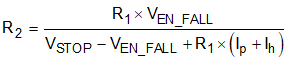
where
- Ip is 0.7 µA.
- Ih is 1.4 µA.
- VEN_FALL is 1.17 .
- VEN_RISE is 1.21 V.
- VSTART is the input voltage enabling the device.
- VSTOP is the input voltage disabling the device.