ZHCSPP3 July 2022 TPS563300
PRODUCTION DATA
- 1 特性
- 2 应用
- 3 说明
- 4 Revision History
- 5 Pin Configuration and Functions
- 6 Specifications
-
7 Detailed Description
- 7.1 Overview
- 7.2 Functional Block Diagram
- 7.3
Feature Description
- 7.3.1 Fixed Frequency Peak Current Mode
- 7.3.2 Pulse Frequency Modulation
- 7.3.3 Voltage Reference
- 7.3.4 Output Voltage Setting
- 7.3.5 Enable and Adjusting Undervoltage Lockout
- 7.3.6 Minimum On Time, Minimum Off Time, and Frequency Foldback
- 7.3.7 Frequency Spread Spectrum
- 7.3.8 Overvoltage Protection
- 7.3.9 Overcurrent and Undervoltage Protection
- 7.3.10 Thermal Shutdown
- 7.4 Device Functional Modes
-
8 Application and Implementation
- 8.1 Application Information
- 8.2
Typical Application
- 8.2.1 Design Requirements
- 8.2.2
Detailed Design Procedure
- 8.2.2.1 Custom Design With WEBENCH® Tools
- 8.2.2.2 Output Voltage Resistors Selection
- 8.2.2.3 Bootstrap Capacitor Selection
- 8.2.2.4 Undervoltage Lockout Set Point
- 8.2.2.5 Output Inductor Selection
- 8.2.2.6 Output Capacitor Selection
- 8.2.2.7 Input Capacitor Selection
- 8.2.2.8 Feedforward Capacitor CFF Selection
- 8.2.2.9 Maximum Ambient Temperature
- 8.2.3 Application Curves
- 8.3 Best Design Practices
- 8.4 Power Supply Recommendations
- 8.5 Layout
- 9 Device and Documentation Support
- 10Mechanical, Packaging, and Orderable Information
7.3.9 Overcurrent and Undervoltage Protection
The TPS563300 incorporates both peak and valley inductor current limits to provide protection to the device from overloads and short circuits and limit the maximum output current. Valley current limit prevents inductor current run-away during short circuits on the output, while both peak and valley limits work together to limit the maximum output current of the converter. Hiccup mode is also incorporated for sustained short circuits.
The high-side switch current is sensed when it is turned on after a set blanking time (tON_MIN), the peak current of high-side switch is limited by the peak current threshold, IHS_LIMIT. The current going through the low-side switch is also sensed and monitored. When the low-side switch turns on, the inductor current begins to ramp down.
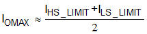
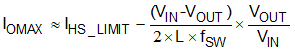
As the device is overloaded, a point is reached where the valley of the inductor current cannot reach below ILS_LIMIT before the next clock cycle, then the low-side switch is kept on until the inductor current ramps below the valley current threshold, ILS_LIMIT, then the low-side switch is turned off and the high-side switch is turned on after a dead time. When this occurs, the valley current limit control skips that cycle, causing the switching frequency to drop. Further overload causes the switching frequency to continue to drop, but the output voltage remains in regulation. As the overload is increased, both the inductor current ripple and peak current increase until the high-side current limit, IHS_LIMIT, is reached. When this limit is tripped, the switch duty cycle is reduced and the output voltage falls out of regulation, which represents the maximum output current from the converter and is given approximately by Equation 9. The output voltage and switching frequency continue to drop as the device moves deeper into overload while the output current remains at approximately IOMAX. If the inductor ripple current is large, the high-side current limit can be tripped before the low-side limit is reached. In this case, Equation 10 gives the approximate maximum output current.
Furthermore, if a severe overload or short circuit causes the FB voltage to fall below VUVP threshold, 65% of the VREF, and triggering current limit, and the condition occurs for more than the hiccup on time (typically 256 μs), the converter enters hiccup mode. In this mode, the device stops switching for hiccup off time, 10.5 × tSS, and then goes to a normal restart with soft-start time. If the overload or short-circuit condition remains, the device runs in current limit and then shuts down again. This cycle repeats as long as the overload or short-circuit condition persists. This mode of operation reduces the temperature rise of the device during a sustained overload or short circuit condition on the output. Once the output short is removed, the output voltage recovers normally to the regulated value.