ZHCSBY9G July 2013 – June 2021 TPS54561
PRODUCTION DATA
- 1 特性
- 2 应用
- 3 说明
- 4 Revision History
- 5 Pin Configuration and Functions
- 6 Specifications
-
7 Detailed Description
- 7.1 Overview
- 7.2 Functional Block Diagram
- 7.3
Feature Description
- 7.3.1 Fixed Frequency PWM Control
- 7.3.2 Slope Compensation Output Current
- 7.3.3 Pulse Skip Eco-mode
- 7.3.4 Low Dropout Operation and Bootstrap Voltage (BOOT)
- 7.3.5 Error Amplifier
- 7.3.6 Adjusting the Output Voltage
- 7.3.7 Enable and Adjusting Undervoltage Lockout
- 7.3.8 Soft Start/Tracking Pin (SS/TR)
- 7.3.9 Sequencing
- 7.3.10 Constant Switching Frequency and Timing Resistor (RT/CLK) Pin)
- 7.3.11 Maximum Switching Frequency
- 7.3.12 Synchronization to RT/CLK Pin
- 7.3.13 Accurate Current Limit Operation
- 7.3.14 Power Good (PWRGD Pin)
- 7.3.15 Overvoltage Protection
- 7.3.16 Thermal Shutdown
- 7.3.17 Small Signal Model for Loop Response
- 7.3.18 Simple Small Signal Model for Peak Current Mode Control
- 7.3.19 Small Signal Model for Frequency Compensation
- 7.4 Device Functional Modes
-
8 Application and Implementation
- 8.1 Application Information
- 8.2
Typical Applications
- 8.2.1
Buck Converter for 7-V to 60-V Input to 5-V at 5-A Output
- 8.2.1.1 Design Requirements
- 8.2.1.2
Detailed Design Procedure
- 8.2.1.2.1 Custom Design with WEBENCH® Tools
- 8.2.1.2.2 Selecting the Switching Frequency
- 8.2.1.2.3 Output Inductor Selection (LO)
- 8.2.1.2.4 Output Capacitor
- 8.2.1.2.5 Catch Diode
- 8.2.1.2.6 Input Capacitor
- 8.2.1.2.7 Slow Start Capacitor
- 8.2.1.2.8 Bootstrap Capacitor Selection
- 8.2.1.2.9 Undervoltage Lockout Set Point
- 8.2.1.2.10 Output Voltage and Feedback Resistors Selection
- 8.2.1.2.11 Compensation
- 8.2.1.2.12 Power Dissipation Estimate
- 8.2.1.2.13 Safe Operating Area
- 8.2.1.2.14 Discontinuous Conduction Mode and Eco-mode Boundary
- 8.2.1.3 Application Curves
- 8.2.2 Inverting Buck-Boost Topology for Positive Input to Negative Output
- 8.2.3 Split-Rail Topology for Positive Input to Negative and Positive Output
- 8.2.1
Buck Converter for 7-V to 60-V Input to 5-V at 5-A Output
- 9 Power Supply Recommendations
- 10Layout
- 11Device and Documentation Support
- 12Mechanical, Packaging, and Orderable Information
7.3.11 Maximum Switching Frequency
To protect the converter in overload conditions at higher switching frequencies and input voltages, the TPS54561 implements a frequency foldback. The oscillator frequency is divided by 1, 2, 4, and 8 as the FB pin voltage falls from 0.8 V to 0 V. The TPS54561 uses a digital frequency foldback to enable synchronization to an external clock during normal start-up and fault conditions. During short-circuit events, the inductor current may exceed the peak current limit because of the high input voltage and the minimum controllable on time. When the output voltage is forced low by the shorted load, the inductor current decreases slowly during the switch off time. The frequency foldback effectively increases the off time by increasing the period of the switching cycle providing more time for the inductor current to ramp down.
With a maximum frequency foldback ratio of 8, there is a maximum frequency at which the inductor current can be controlled by frequency foldback protection. Equation 13 calculates the maximum switching frequency at which the inductor current will remain under control when VOUT is forced to VOUT(SC). The selected operating frequency should not exceed the calculated value.
Equation 12 calculates the maximum switching frequency limitation set by the minimum controllable on time and the input to output step down ratio. Setting the switching frequency above this value will cause the regulator to skip switching pulses to achieve the low duty cycle required to regulate the output at maximum input voltage.
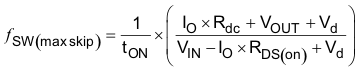
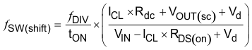
| IO | Output current |
| ICL | Current limit |
| Rdc | Inductor resistance |
| VIN | Maximum input voltage |
| VOUT | Output voltage |
| VOUT(SC) | Output voltage during short |
| Vd | Diode voltage drop |
| RDS(on) | Switch on resistance |
| tON | Controllable on time |
| ƒDIV | Frequency divide equals (1, 2, 4, or 8) |