ZHCSBY9G July 2013 – June 2021 TPS54561
PRODUCTION DATA
- 1 特性
- 2 应用
- 3 说明
- 4 Revision History
- 5 Pin Configuration and Functions
- 6 Specifications
-
7 Detailed Description
- 7.1 Overview
- 7.2 Functional Block Diagram
- 7.3
Feature Description
- 7.3.1 Fixed Frequency PWM Control
- 7.3.2 Slope Compensation Output Current
- 7.3.3 Pulse Skip Eco-mode
- 7.3.4 Low Dropout Operation and Bootstrap Voltage (BOOT)
- 7.3.5 Error Amplifier
- 7.3.6 Adjusting the Output Voltage
- 7.3.7 Enable and Adjusting Undervoltage Lockout
- 7.3.8 Soft Start/Tracking Pin (SS/TR)
- 7.3.9 Sequencing
- 7.3.10 Constant Switching Frequency and Timing Resistor (RT/CLK) Pin)
- 7.3.11 Maximum Switching Frequency
- 7.3.12 Synchronization to RT/CLK Pin
- 7.3.13 Accurate Current Limit Operation
- 7.3.14 Power Good (PWRGD Pin)
- 7.3.15 Overvoltage Protection
- 7.3.16 Thermal Shutdown
- 7.3.17 Small Signal Model for Loop Response
- 7.3.18 Simple Small Signal Model for Peak Current Mode Control
- 7.3.19 Small Signal Model for Frequency Compensation
- 7.4 Device Functional Modes
-
8 Application and Implementation
- 8.1 Application Information
- 8.2
Typical Applications
- 8.2.1
Buck Converter for 7-V to 60-V Input to 5-V at 5-A Output
- 8.2.1.1 Design Requirements
- 8.2.1.2
Detailed Design Procedure
- 8.2.1.2.1 Custom Design with WEBENCH® Tools
- 8.2.1.2.2 Selecting the Switching Frequency
- 8.2.1.2.3 Output Inductor Selection (LO)
- 8.2.1.2.4 Output Capacitor
- 8.2.1.2.5 Catch Diode
- 8.2.1.2.6 Input Capacitor
- 8.2.1.2.7 Slow Start Capacitor
- 8.2.1.2.8 Bootstrap Capacitor Selection
- 8.2.1.2.9 Undervoltage Lockout Set Point
- 8.2.1.2.10 Output Voltage and Feedback Resistors Selection
- 8.2.1.2.11 Compensation
- 8.2.1.2.12 Power Dissipation Estimate
- 8.2.1.2.13 Safe Operating Area
- 8.2.1.2.14 Discontinuous Conduction Mode and Eco-mode Boundary
- 8.2.1.3 Application Curves
- 8.2.2 Inverting Buck-Boost Topology for Positive Input to Negative Output
- 8.2.3 Split-Rail Topology for Positive Input to Negative and Positive Output
- 8.2.1
Buck Converter for 7-V to 60-V Input to 5-V at 5-A Output
- 9 Power Supply Recommendations
- 10Layout
- 11Device and Documentation Support
- 12Mechanical, Packaging, and Orderable Information
8.2.1.2.3 Output Inductor Selection (LO)
To calculate the minimum value of the output inductor, use Equation 31.
KIND is a ratio that represents the amount of inductor ripple current relative to the maximum output current. The inductor ripple current is filtered by the output capacitor. Therefore, choosing high inductor ripple currents impacts the selection of the output capacitor since the output capacitor must have a ripple current rating equal to or greater than the inductor ripple current. In general, the inductor ripple value is at the discretion of the designer, however, the following guidelines may be used.
For designs using low ESR output capacitors such as ceramics, a value as high as KIND = 0.3 may be desirable. When using higher ESR output capacitors, KIND = 0.2 yields better results. Since the inductor ripple current is part of the current mode PWM control system, the inductor ripple current should always be greater than 150 mA for stable PWM operation. In a wide input voltage regulator, it is best to choose relatively large inductor ripple current. This provides sufficienct ripple current with the input voltage at the minimum.
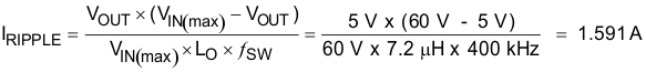
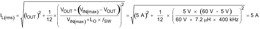
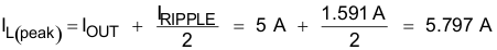
For this design example, KIND = 0.3 and the inductor value is calculated to be 7.6 μH. The nearest standard value is 7.2 μH. It is important that the RMS current and saturation current ratings of the inductor not be exceeded. The RMS and peak inductor current can be found from Equation 33 and Equation 34. For this design, the RMS inductor current is 5 A and the peak inductor current is 5.8 A. The chosen inductor is a WE 7447798720, which has a saturation current rating of 7.9 A and an RMS current rating of 6 A.
As the equation set demonstrates, lower ripple currents will reduce the output voltage ripple of the regulator but will require a larger value of inductance. Selecting higher ripple currents will increase the output voltage ripple of the regulator but allow for a lower inductance value.
The current flowing through the inductor is the inductor ripple current plus the output current. During power up, faults or transient load conditions, the inductor current can increase above the peak inductor current level calculated above. In transient conditions, the inductor current can increase up to the switch current limit of the device. For this reason, the most conservative design approach is to choose an inductor with a saturation current rating equal to or greater than the switch current limit of the TPS54561 which is nominally 7.5 A.