ZHCSBY9G July 2013 – June 2021 TPS54561
PRODUCTION DATA
- 1 特性
- 2 应用
- 3 说明
- 4 Revision History
- 5 Pin Configuration and Functions
- 6 Specifications
-
7 Detailed Description
- 7.1 Overview
- 7.2 Functional Block Diagram
- 7.3
Feature Description
- 7.3.1 Fixed Frequency PWM Control
- 7.3.2 Slope Compensation Output Current
- 7.3.3 Pulse Skip Eco-mode
- 7.3.4 Low Dropout Operation and Bootstrap Voltage (BOOT)
- 7.3.5 Error Amplifier
- 7.3.6 Adjusting the Output Voltage
- 7.3.7 Enable and Adjusting Undervoltage Lockout
- 7.3.8 Soft Start/Tracking Pin (SS/TR)
- 7.3.9 Sequencing
- 7.3.10 Constant Switching Frequency and Timing Resistor (RT/CLK) Pin)
- 7.3.11 Maximum Switching Frequency
- 7.3.12 Synchronization to RT/CLK Pin
- 7.3.13 Accurate Current Limit Operation
- 7.3.14 Power Good (PWRGD Pin)
- 7.3.15 Overvoltage Protection
- 7.3.16 Thermal Shutdown
- 7.3.17 Small Signal Model for Loop Response
- 7.3.18 Simple Small Signal Model for Peak Current Mode Control
- 7.3.19 Small Signal Model for Frequency Compensation
- 7.4 Device Functional Modes
-
8 Application and Implementation
- 8.1 Application Information
- 8.2
Typical Applications
- 8.2.1
Buck Converter for 7-V to 60-V Input to 5-V at 5-A Output
- 8.2.1.1 Design Requirements
- 8.2.1.2
Detailed Design Procedure
- 8.2.1.2.1 Custom Design with WEBENCH® Tools
- 8.2.1.2.2 Selecting the Switching Frequency
- 8.2.1.2.3 Output Inductor Selection (LO)
- 8.2.1.2.4 Output Capacitor
- 8.2.1.2.5 Catch Diode
- 8.2.1.2.6 Input Capacitor
- 8.2.1.2.7 Slow Start Capacitor
- 8.2.1.2.8 Bootstrap Capacitor Selection
- 8.2.1.2.9 Undervoltage Lockout Set Point
- 8.2.1.2.10 Output Voltage and Feedback Resistors Selection
- 8.2.1.2.11 Compensation
- 8.2.1.2.12 Power Dissipation Estimate
- 8.2.1.2.13 Safe Operating Area
- 8.2.1.2.14 Discontinuous Conduction Mode and Eco-mode Boundary
- 8.2.1.3 Application Curves
- 8.2.2 Inverting Buck-Boost Topology for Positive Input to Negative Output
- 8.2.3 Split-Rail Topology for Positive Input to Negative and Positive Output
- 8.2.1
Buck Converter for 7-V to 60-V Input to 5-V at 5-A Output
- 9 Power Supply Recommendations
- 10Layout
- 11Device and Documentation Support
- 12Mechanical, Packaging, and Orderable Information
8.2.1.2.12 Power Dissipation Estimate
The following formulas show how to estimate the TPS54561 power dissipation under continuous conduction mode (CCM) operation. These equations should not be used if the device is operating in discontinuous conduction mode (DCM).
The power dissipation of the IC includes conduction loss (PCOND), switching loss (PSW), gate drive loss (PGD) and supply current (PQ). Example calculations are shown with the 12-V typical input voltage of the design example.


Where:
IOUT is the output current (A).
RDS(on) is the on-resistance of the high-side MOSFET (Ω).
VOUT is the output voltage (V).
VIN is the input voltage (V).
fsw is the switching frequency (Hz).
trise is the SW pin voltage rise time and can be estimated by trise = VIN x 0.16 ns/V + 3 ns
QG is the total gate charge of the internal MOSFET
IQ is the operating nonswitching supply current
Therefore,

For given TA,
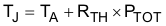
For given TJMAX = 150°C
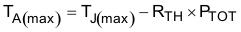
Where:
Ptot
is the total device power dissipation (W).
TA is the ambient temperature (°C).
TJ is the junction temperature (°C).
RTH is the thermal resistance from junction to ambient for a given
PCB layout (°C/W).
TJMAX is maximum
junction temperature (°C).
TAMAX is
maximum ambient temperature (°C).
There will be additional power losses in the regulator circuit due to the inductor ac and dc losses, the catch diode and PCB trace resistance impacting the overall efficiency of the regulator.