ZHCSBY9G July 2013 – June 2021 TPS54561
PRODUCTION DATA
- 1 特性
- 2 应用
- 3 说明
- 4 Revision History
- 5 Pin Configuration and Functions
- 6 Specifications
-
7 Detailed Description
- 7.1 Overview
- 7.2 Functional Block Diagram
- 7.3
Feature Description
- 7.3.1 Fixed Frequency PWM Control
- 7.3.2 Slope Compensation Output Current
- 7.3.3 Pulse Skip Eco-mode
- 7.3.4 Low Dropout Operation and Bootstrap Voltage (BOOT)
- 7.3.5 Error Amplifier
- 7.3.6 Adjusting the Output Voltage
- 7.3.7 Enable and Adjusting Undervoltage Lockout
- 7.3.8 Soft Start/Tracking Pin (SS/TR)
- 7.3.9 Sequencing
- 7.3.10 Constant Switching Frequency and Timing Resistor (RT/CLK) Pin)
- 7.3.11 Maximum Switching Frequency
- 7.3.12 Synchronization to RT/CLK Pin
- 7.3.13 Accurate Current Limit Operation
- 7.3.14 Power Good (PWRGD Pin)
- 7.3.15 Overvoltage Protection
- 7.3.16 Thermal Shutdown
- 7.3.17 Small Signal Model for Loop Response
- 7.3.18 Simple Small Signal Model for Peak Current Mode Control
- 7.3.19 Small Signal Model for Frequency Compensation
- 7.4 Device Functional Modes
-
8 Application and Implementation
- 8.1 Application Information
- 8.2
Typical Applications
- 8.2.1
Buck Converter for 7-V to 60-V Input to 5-V at 5-A Output
- 8.2.1.1 Design Requirements
- 8.2.1.2
Detailed Design Procedure
- 8.2.1.2.1 Custom Design with WEBENCH® Tools
- 8.2.1.2.2 Selecting the Switching Frequency
- 8.2.1.2.3 Output Inductor Selection (LO)
- 8.2.1.2.4 Output Capacitor
- 8.2.1.2.5 Catch Diode
- 8.2.1.2.6 Input Capacitor
- 8.2.1.2.7 Slow Start Capacitor
- 8.2.1.2.8 Bootstrap Capacitor Selection
- 8.2.1.2.9 Undervoltage Lockout Set Point
- 8.2.1.2.10 Output Voltage and Feedback Resistors Selection
- 8.2.1.2.11 Compensation
- 8.2.1.2.12 Power Dissipation Estimate
- 8.2.1.2.13 Safe Operating Area
- 8.2.1.2.14 Discontinuous Conduction Mode and Eco-mode Boundary
- 8.2.1.3 Application Curves
- 8.2.2 Inverting Buck-Boost Topology for Positive Input to Negative Output
- 8.2.3 Split-Rail Topology for Positive Input to Negative and Positive Output
- 8.2.1
Buck Converter for 7-V to 60-V Input to 5-V at 5-A Output
- 9 Power Supply Recommendations
- 10Layout
- 11Device and Documentation Support
- 12Mechanical, Packaging, and Orderable Information
7.3.9 Sequencing
Many of the common power supply sequencing methods can be implemented using the SS/TR, EN, and PWRGD pins. The sequential method can be implemented using an open drain output of a power on reset pin of another device. The sequential method is illustrated in Figure 7-4 using two TPS54561 devices. The power good is Connected to the EN pin on the TPS54561 which will enable the second power supply once the primary supply reaches regulation. If needed, a 1-nF ceramic capacitor on the EN pin of the second power supply will provide a 1-ms start up delay. Figure 7-5 shows the results of Figure 7-4.
 Figure 7-4 Schematic for Sequential Start-Up Sequence
 Figure 7-5 Sequential Startup using EN and PWRGD
 Figure 7-6 Schematic for Ratio-Metric Start-Up Sequence
 Figure 7-7 Ratio-Metric Startup using Coupled SS/TR pins
Figure 7-6 shows a method for ratio-metric start up sequence by connecting the SS/TR pins together. The regulator outputs will ramp up and reach regulation at the same time. When calculating the soft start time the pull up current source must be doubled in Equation 5. Figure 7-7 shows the results of Figure 7-6.
 Figure 7-8 Schematic for Ratio-Metric and Simultaneous Start-Up Sequence
Ratio-metric and simultaneous power supply sequencing can be implemented by connecting the resistor network of R1 and R2 shown in Figure 7-8 to the output of the power supply that needs to be tracked or another voltage reference source. Using Equation 6 and Equation 7, the tracking resistors can be calculated to initiate the Vout2 slightly before, after or at the same time as Vout1. Equation 8 is the voltage difference between Vout1 and Vout2 at the 95% of nominal output regulation.
The deltaV variable is zero volts for simultaneous sequencing. To minimize the effect of the inherent SS/TR to FB offset (VSSOFFSET) in the soft start circuit and the offset created by the pullup current source (Iss) and tracking resistors, the VSSOFFSET and ISS are included as variables in the equations.
To design a ratio-metric start up in which the Vout2 voltage is slightly greater than the Vout1 voltage when Vout2 reaches regulation, use a negative number in Equation 6 through Equation 8 for deltaV. Equation 8 will result in a positive number for applications which the Vout2 is slightly lower than Vout1 when Vout2 regulation is achieved.
Since the SS/TR pin must be pulled below 54 mV before starting after an EN, UVLO or thermal shutdown fault, careful selection of the tracking resistors ensures that the device will restart after a fault. The calculated R1 value from Equation 6 must be greater than the value calculated in Equation 9 to ensure the device recovers from a fault.
As the SS/TR voltage becomes more than 85% of the nominal reference voltage the VSSOFFSET becomes larger as the soft start circuits gradually handoff the regulation reference to the internal voltage reference. The SS/TR pin voltage needs to be greater than 1.5 V for a complete handoff to the internal voltage reference.
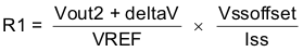
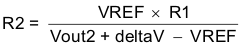
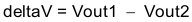

 Figure 7-9 Ratio-Metric Startup with Tracking Resistors
 Figure 7-11 Simultaneous Startup with Tracking Resistor
 Figure 7-10 Ratio-Metric Startup with Tracking Resistors